SSZTBM7 February 2016 TL494
When I started working on designing a pulse width modulator for my LED driver, there were two things I knew from the start: that the light-emitting diode (LED) driver needed a pulse-width modulated (PWM) signal and that I wanted to use hardware. I remembered that the test circuit in the TL494 data sheet shows a PWM generator circuit (see Figure 1) that needs minimal components for a very low bill-of-materials cost. The TL494 has many useful circuits inside: two amplifiers, an oscillator, comparator, flip-flop and two high-current outputs that can sink or source current. See Figure 2. Today I will use my LED driver as an example to explain how to use error amplifiers to remove error and variance.
 Figure 1 The TL494 Data Sheet’s
Operational Test Circuit and Waveforms
Figure 1 The TL494 Data Sheet’s
Operational Test Circuit and Waveforms Figure 2 Functional Block Diagram
for the TL494
Figure 2 Functional Block Diagram
for the TL494I have two choices for modulation input: the dead-time-control (DTC) or FEEDBACK pin. I chose the FEEDBACK pin input because I can use one of the TL494’s two internal error amplifiers to scale my input signal to match the device’s feedback voltage range.
The only changes I made to the circuit in Figure 1 was to set pin 13 to ground and to replace the 12kΩ resistor with 6.8kΩ. Now, duty-cycle output can be up to 90% and the output frequency is 18kHz.
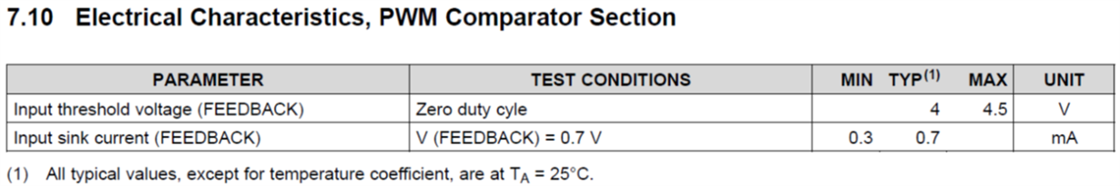
I know that maximum duty cycle occurs when FEEDBACK is 0.7V (per Figure 1) and that zero duty cycle is typically 4V, per Table 1.
|
I built the circuit in Figure 1 and recorded the relationship between the FEEDBACK voltage and output duty cycle using an oscilloscope. The maximum duty cycle is 88% and the minimum duty cycle is 4%, with FEEDBACK between 1.1V and 3.4V, as shown in Figure 3.
 Figure 3 Relationship between FEEDBACK
Voltage and Output Duty Cycle
Figure 3 Relationship between FEEDBACK
Voltage and Output Duty CycleI started to wonder how device-to-device variance for FEEDBACK and duty cycle might vary. I put that thought aside, however, and decided to check temperature performance first. I was surprised to find out that the actual duty cycle varied significantly from the desired duty cycle as the temperature changed. The duty cycle at low and high temperature changed as much as 4% from the result recorded in Figure 3. The duty cycle deviation due to temperature is shown in Figure 4. The shift is most serious when a small duty cycle is needed, such as 4%. Across temperature, the duty cycle will vary from 1.5% at -40°C to 5.8% at 85°C.This will be a substantial difference in LED brightness.
On the plus side, I was happy with temperature stability of the oscillator frequency shown in Figure 5.
 Figure 4 Shift in Output Duty Cycle
vs. Desired Duty Cycle for Five Different Temperatures
Figure 4 Shift in Output Duty Cycle
vs. Desired Duty Cycle for Five Different Temperatures Figure 5 Output Frequency versus
Temperature
Figure 5 Output Frequency versus
TemperatureI needed a way to control the output duty cycle that would be immune from temperature effects of the FEEDBACK-to-duty-cycle relationship and device-to-device variance that I expected would cause even greater variance in duty cycle. After some thought, it occurred to me that converting the duty cycle of the output to a voltage and comparing that voltage to my input would result in a duty cycle equal to my input voltage. The easiest way to convert the duty cycle of a PWM signal to a DC voltage is with a low-pass filter. I used the internal error amplifier to compare the signals. To avoid adding new sources of error, the PWM signal going to the low-pass-filter should have accurate and unchanging low and high output voltage levels. Many logic inverters have rail-to-rail output making them a good choice, but I went with a NPN transistor based inverter instead, which also has a rail-to-rail output. Figure 6 shows the new circuit.
There are design changes you should consider. As always, resistor and capacitor on the TL494’s RT and CT pins set the oscillator frequency. R3 multiplied by C3 in the low pass filter needs to be at least three times the oscillator time base to convert the duty cycle to a DC voltage. R2 and C2 control the frequency compensation for the control loop. Larger values for C2 and C3 can keep the ripple voltage to a minimum, while lower values allow for higher modulation frequencies of the input signal. The low output voltage at the TL494’s C1 pin doesn’t go all the way to ground; therefore you will need the resistor divider using R5 and R7.
 Figure 6 New Schematic to Regulate
Output Duty Cycle
Figure 6 New Schematic to Regulate
Output Duty CycleSending the duty-cycle information back to the error amplifier shown in Figure 6 reduces the difference between the actual duty cycle and the desired duty cycle, as Figure 7 shows. The error dropped to 0.2%, which is very good considering that the oscilloscope has a 0.1% resolution for its duty-cycle measurement.
 Figure 7 Shift in Output Duty Cycle vs.
Desired Duty Cycle for Five Different Temperatures
Figure 7 Shift in Output Duty Cycle vs.
Desired Duty Cycle for Five Different TemperaturesError amplifiers are a good way to remove error and variance from both simple and complex input to output relationships. Now, my LED driver duty-cycle will be accurate across temperature and from device to device.
Additional Resources
- Join the TI E2E™ Community Non-Isolated DC/DC forum.
- Read more blogs about LED technology.
- Start a power supply design with WEBENCH Design and Simulation Tools.
- Search TI high-speed op amps and find technical resources