SSZTBK6 march 2016 LMX2582 , LMX2592
If you’re like me, you may find some specifications in a typical datasheet hard to read because they include an implied convention with which you aren’t familiar. One such specification for many RF system engineers is phase noise in a phase-locked loop (PLL). Phase noise performance can make all the difference in meeting your system requirements when your signal source is used as a local oscillator (LO) or as a high speed clock. Extracting this specification in a data sheet can seem like a project in itself at first. Let me explain how to read the phase noise specifications of a PLL to help you make a first cut assessment of the attainable performance for your radio or high-speed application.
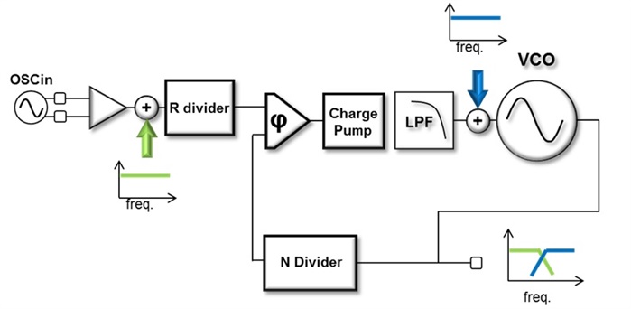
Remember that a PLL is a control loop and such a system has a frequency response. Noise generated in the reference path is subject to the loop’s low-pass frequency response to the output of the system, while noise generated in the voltage-controlled oscillator (VCO) path is subject to the loop’s high-pass frequency response to the output of the system. See Figure 1.
 Figure 1 Two Modeled Noise Sources
(Green and Blue) in a Phase-locked Loop and Their Frequency Response to System
Output
Figure 1 Two Modeled Noise Sources
(Green and Blue) in a Phase-locked Loop and Their Frequency Response to System
OutputNoise generated by the PLL inside the loop bandwidth (the low-pass frequency response) is divided into two components – flicker noise and flat noise – while noise outside the loop bandwidth (the high-pass frequency response) is typically described by the open-loop VCO performance in the data sheet.
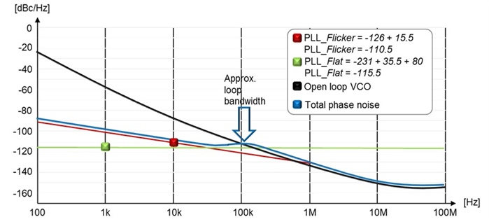
These specifications together impact total phase noise when inserted in the loop dynamic. Figure 2 shows how the three noise specifications define total phase noise for an approximate selected loop bandwidth. Notice how the total phase noise is tracking the VCO above the loop bandwidth and tracking the PLL below the loop bandwidth.
 Figure 2 Estimated Phase Noise Plot of
the LMX2592 for a 6-GHz Output with a 100-MHz Phase Detector Frequency Using (1)
Flicker Noise, (2) Flat Noise and (3) VCO Open-loop Data for a ~100-kHz Loop
Bandwidth.
Figure 2 Estimated Phase Noise Plot of
the LMX2592 for a 6-GHz Output with a 100-MHz Phase Detector Frequency Using (1)
Flicker Noise, (2) Flat Noise and (3) VCO Open-loop Data for a ~100-kHz Loop
Bandwidth.Let’s briefly review the three specifications:
1) Flicker Noise
(the red line in Figure 2) is a characteristic of the phase-locked loop and impacts phase noise at lower offsets. This noise changes at a rate of 10 dB per decade with respect to the offset frequency. TI specifies that noise and normalizes it for a 1-GHz carrier at a 10-kHz offset. Equation Figure 1 de- normalizes flicker noise as:
 Figure 3 (1)
where Fvco is the frequency of the VCO.
Flicker noise is in general independent of the phase-detector frequency and depends on the output carrier frequency only. Hence, doubling the output frequency will increase the noise by 6 dB.
2) Flat Noise
(the green line in Figure 2) is also called the figure of merit of the phase-locked loop and is normalized for comparison purposes. The unit of the figure of merit is in decibel compared to the output signal in a 1-Hz bandwidth [dBc/Hz] at a carrier of 1 Hz. There is no frequency offset specified, as this is a flat noise. Equation Figure 1 denormalizes flat noise as:
 Figure 4 (2)
where N is the divider of the feedback (see Figure 1) and Fpd is the running frequency of the phase detector.
This specification will impact the phase noise at middle offset frequencies. As you can see from Equation Figure 1, the higher phase-detector frequency provides better phase noise inside the loop by 3dB each time the phase-detector frequency doubles.
3) Open-loop VCO Phase Noise
(the black line in Figure 2) typically follows a 20 dB per decade relationship with offset frequency; however closer to the carrier it changes to 30 dB per decade. Noise is flat, typically passed 15 or 20-MHz offset frequency, and is called the noise floor of the source. The noise from the VCO in the phase-locked loop goes into a high-pass frequency response. Finally, the phase noise typically scales with the output frequency so that half the frequency will improve the phase noise by 6 dB.
You can now get the approximate phase noise of your PLL at different offset frequency and output frequencies. You need to get from the datasheet the flicker noise, the flat noise and the open loop VCO phase noise. You then denormalize these specifications with Equation Figure 1 and Figure 1 and you can approximate the closed loop response by assuming a very sharp loop filter as a first approximation as shown in Figure 2.
Estimating PLL phase noise seems challenging at first, but extracting the needed specifications in the data sheet and using the formulas outlined here will help you to select the best PLL to meet your system requirements. For an accurate simulation, we also offers two tools to calculate the phase noise of your PLL: WEBENCH® Clock Architect and PLLatinum™ Sim. You can learn about the LMX2592 and TI’s other RF PLLs and synthesizers as well as explores these tools on this page.
Additional Resources
- Explore the datasheets of the new wideband RF PLLs with integrated VCO: LMX2592 and LMX2582.
- Read other Analog technical articles about designing with PLLs.