SSZTB97 may 2016 ADC32RF45 , LMX2582
** This is the 11th post in an Analog Wire RF-sampling blog series. **
I discussed the benefits of the radio frequency (RF) sampling architecture for wide-bandwidth systems in a previous post, however, the analog-to-digital converter (ADC) is often the limiting component for supporting large signal bandwidths in receiver systems. In this post, I will discuss how to push your wideband telecommunication systems past 1GHz.
Why do you need receivers capable of such wide bandwidths? For telecommunication service providers, wider bandwidths increase their system capacity and data throughput.They require improvements over existing systems, because the number of cellular users is expected to exceed 5 billion by 2019. At the same time, users demand more data services to connect with social media, transfer work files, and stream video.
To meet customer demand, providers utilize carrier aggregation systems to spread signals across multiple bands in order to access additional bandwidth. 5G cellular systems will use wide-bandwidth signals in the microwave frequency bands, where a lot of unused spectrum is available.
Digital pre-distortion (DPD) feedback receivers also need large signal bandwidths. DPD generally requires an increase in the transmitted signal bandwidth to compensate for the third- and fifth-order intermodulation products generated in the power amplifier (PA). As transmittersignal bandwidth increases, the DPD signal bandwidth expands fivefold. An RF sampling ADC is the key component in all of these systems.
Yet bandwidth alone is not sufficient. High-end telecommunication systems require a high dynamic range. The receiver must handle both high- and low-signal levels.
Figure 1 illustrates a potential receiver spectrum with the desired frequency channel, along with a narrowband interferer and the transmitter bleedthrough signal. The interferer falls within the channel filter bandwidth; the ADC must handle that high signal without saturating. The duplexer filter and channel filter highly attenuate the transmitter signal – but since it starts out at a very high power level, it is still significant by the time it reaches the ADC input. If those interferers fall at the proper frequency, the intermodulation product lands right on the desired signal.
Additionally, the interferer’s high-order harmonics may fold back onto the desired channel. A high-linearity ADC with excellent spurious free dynamic range (SFDR) minimizes the degradation impact in these blocking scenarios.
 Figure 1 Receiver Interference
Spectrum
Figure 1 Receiver Interference
SpectrumOn the other end of the scale, you want a low noise floor to discern small signals from the noise. The noise figure of the system determines the receiver sensitivity. The sensitivity level is the lowest signal from which the receiver can extract the desired information. The ADC’s signal-to-noise ratio (SNR) indicates the noise level in relation to a high input signal (usually near full-scale input). The absolute noise power density with a low-level signal indicates the device’s minimum noise-floor limit.
The thermal noise performance of the device is fixed. There is also noise contribution from the clock jitter. The total jitter is the root mean square (RMS) of the external clock jitter and the aperture jitter as seen in equation 1. The aperture jitter is fixed and is inherent to the device; the value is extracted from the device’s datasheet. The clock jitter depends on the designer’s external clock choice. Implementing a low jitter clock solution is critical for good SNR performance. Equation 2 expresses how jitter impacts SNR:
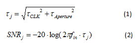
Notice that the sampling frequency is not part of the equation, however, the input frequency is included. RF sampling converters are not inherently more sensitive to clock jitter, but because they operate at higher frequencies, clock jitter becomes a key factor in SNR performance.
There is a need to support the dynamic range of high-end receiver systems and very wide signal bandwidths. The TI Designs 1-GHz Signal Bandwidth RF Sampling Receiver Reference Design (TIDA-01161) showcases a solution for a 1GHz bandwidth signal suitable for stringent telecommunication standards. The ADC32RF45 is a 14-bit, dual-channel, 3GSPS ADC. It has a 3dB input bandwidth of 3GHz and samples input signals up to 4GHz. The device supports signal bandwidths of over 1GHz (up to 1.5GHz maximum).
Figure 2 shows a captured 1GHz-wide signal. The signal includes a total of 40 20MHz-wide cellular long term evolution (LTE) carriers (4G) centered at 2.2GHz. Four groups are separated by about 65MHz, with 10 carriers per group. The entire signal-bandwidth power is about -30dBFS. Notice that the spectrum is quite clean and that the noise floor is about -100dBFS, which is limited by the input signal’s noise.
 Figure 2 1GHz-wide Signal Bandwidth
Captured by the ADC32RF45 ADC
Figure 2 1GHz-wide Signal Bandwidth
Captured by the ADC32RF45 ADCThis reference design uses both the ADC32RF45 and the LMX2582 RF synthesizer for the ADC clock. The LMX2582 achieves a phase noise of -140dBc/Hz at 3GHz. This performance rivals test equipment and is suitable as a clock source for high-end RF sampling converters. This system is usable for wireless infrastructure base station receivers, large radar antenna arrays, high-end test equipment and DPD feedback receivers.
Next generation receivers need high dynamic range and large bandwidth capabilities to meet the growing capacity demands and the increase in data services. The RF sampling architecture meets those requirements, while effectively integrating the functions of several other blocks which compacts the design. This translates to lower cost and easier to design systems.
Check back next month when I discuss the RF sampling advantages when using integrated digital down converters.
Additional Resources
- Visit the High Speed Signal Chain University to watch the RF sampling video series.
- Search for solutions, ask questions and solve problems in the TI E2E™ Community High Speed Data Converter forum.
- Visit TI’s RF sampling page for a full suite of support resources, including TI Designs reference designs and application notes.
- See other posts in Russell’s RF sampling blog series.
- Learn about TI’s data converter portfolio and find technical resources.