SSZTAY1 september 2016 OPA855 , OPA858 , OPA859
In the first installment of this series, I described various factors that affect the loop gain of a transimpedance amplifier (TIA) and demonstrated how to compensate a TIA to achieve a Butterworth (maximally flat) closed-loop response. In this installment, I will show you how to compensate a TIA for an arbitrary phase margin.
The closed-form equations to determine the closed-loop bandwidth and feedback capacitance (CF) for TIA compensation can be quite involved. A simpler approach is to first compensate the TIA for a Butterworth response (Q = 0.707) using the theory presented in part 1 of this series and then, using Figure 1 below, determine the CF to achieve the desired quality factor (Q). Figure 1 also gives the resulting closed-loop bandwidth of the amplifier for the desired Q factor.
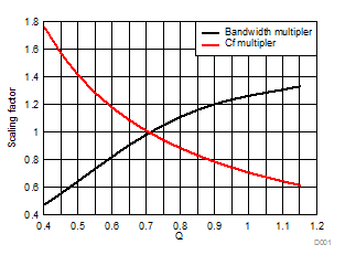 Figure 1 Scaling Factor for Bandwidth
(F - 3dB) and CF Vs. Q Factor
Figure 1 Scaling Factor for Bandwidth
(F - 3dB) and CF Vs. Q FactorUsing the example for a Butterworth response from part 1 of this series, set CF = 0.14pF, which results in f-3dB = 10MHz. To achieve a Q = 0.6, from Figure 1 the resulting CF = 0.14pF x 1.190 = 0.17pF and the resulting f-3dB = 10MHz x 0.82 = 8.2MHz.
For more accurate results, you can download this Excel spreadsheet from the TI E2E™ Community. Figure 2 is a screenshot of two calculators in the spreadsheet. Calculators A and B determine the value of both f-3dB and CF for a Butterworth response and an arbitrary value of Q, respectively.
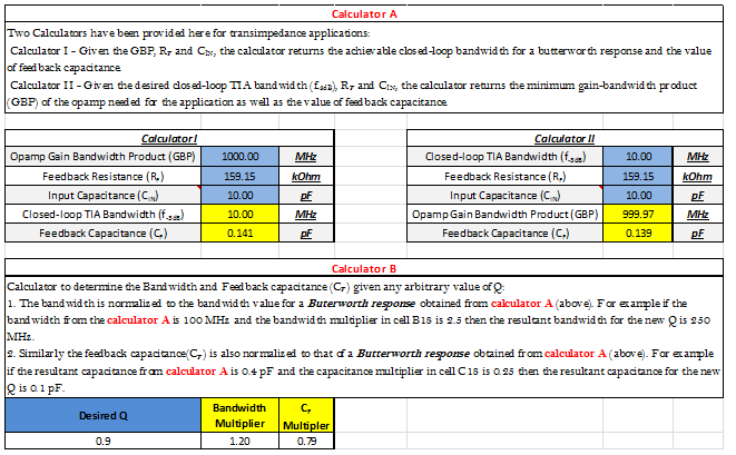 Figure 2 Excel Calculators to Aid in
TIA Design
Figure 2 Excel Calculators to Aid in
TIA DesignThe Q of a circuit is directly related to its phase margin (ΦM), which determines the amplifier’s closed-loop frequency response and time-domain pulse response. An amplifier circuit with a low phase margin has a peaked frequency response and significant ringing in the pulse response. Conversely, a circuit with high phase margin has a flat frequency response and little or no overshoot in the pulse response.
Circuits with low phase margin extend the amplifier’s closed-loop bandwidth, while circuits with high phase margin reduce the closed-loop bandwidth. A Butterworth response, which has a Q = 0.707 and a maximally flat frequency response, has a phase margin of 65.5 degrees and about 4.3% overshoot in the pulse response. Figure 3 shows the Q and overshoot as a function of phase margin.
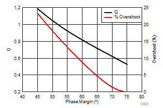 Figure 3 Q and Overshoot vs. Phase
Margin
Figure 3 Q and Overshoot vs. Phase
MarginTo simplify the circuit design, the Excel spreadsheet also has Calculator C, with three separate calculators showing the relationships between Q, overshoot, phase margin and frequency-response peaking.
Calculator C1 gives the phase margin and overshoot for a given value of Q.
Calculator C2 calculates the Q and overshoot for a given value of phase margin. This calculator is useful for achieving a desired frequency-response shape for stability and for maximizing flatness in narrowband applications.
Calculator C3 is useful in time-domain applications when you want to target a certain value of overshoot in the pulse response.
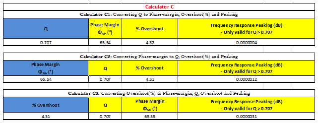 Figure 4 Calculator C Relating Q, Phase
Margin and Overshoot
Figure 4 Calculator C Relating Q, Phase
Margin and OvershootUsing the three different calculators, I calculated the frequency- and time-domain responses for the TIA discussed in part 1 of this series for different values of Q:
- Calculator A produced the CF and f-3dB for a Butterworth response with the specified op amp transimpedance gain and input capacitance.
- Calculator B gave the scaling factor for CF and the change in f-3dB for different values of Q.
- Calculator C predicted the peaking in the frequency response and the overshoot in the pulse response.
The simulated results in Figure 5 match the calculated values very closely.
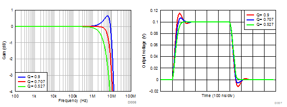 Figure 5 Simulated Closed-loop
Frequency and Transient Responses as a Function of Q
Figure 5 Simulated Closed-loop
Frequency and Transient Responses as a Function of QYou should now be very comfortable with compensating a TIA based on the specific application requirements. The calculators introduced in this post are intended for use with TINA-TI™ software to provide a starting point for TIA design. In the next installment of this series, I will describe the effects of the amplifier’s higher-order open-loop poles on the loop gain of a TIA and introduce the concept of decompensated amplifiers.
Additional Resources
- Get online support in the TI E2E™ Community Amplifier forums.
- Read the first installment of this series, “What you need to know about transimpedance amplifiers – part 1.”
- Download a free version of TINA-TI software.
- Learn about TI’s entire portfolio of amplifier ICs and find technical resources.