SSZTAX3 september 2016 DS125DF1610
Welcome back to the “Eye Doctor” series! In the first installment, I highlighted the problems that can result from over-equalizing a signal. In this installment, I’d like to talk about another common signal-integrity issue: reflections and common ways to mitigate reflections.
Transmission line theory tells us that reflections arise from any change in impedance that the signal may encounter between the output of the source all the way down to the input of the receiving component. Essentially, when an alternating current (AC) signal encounters a change in impedance while traveling down a transmission line, some of the signal is reflected back to the transmitter, while the rest of the signal continues towards the receiver. The greater the impedance change experienced by the signal, the greater the reflection and thus more signal distortion.
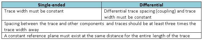
Impedance changes are caused by changes to trace width, spacing between adjacent traces and components, and distance to the reference plane. However, it isn’t always obvious where these impedance changes occur in a printed circuit board (PCB). A very useful practice is to inspect the PCB layout or system diagram to quickly identify any trouble areas that could require more investigation through simulation. When performing this type of inspection, you should trace the signal from the source to the receiver, looking for any violation of the guidelines listed in Table 1 and trouble areas I’ll discuss next.
|
It is not always possible to adhere to the guidelines in Table 1 for transmission lines. Here are some common areas where violations of these guidelines may occur:
- Ball grid array (BGA) routing – especially for large input/output (I/O) count devices that route to inner rows/columns.
- Vias, where you must take extra care to ensure that the transmission line signal vias see a constant fixed reference plane as they travel through the PCB layers.
- In-line components and connectors. Printed circuit board (PCB) footprints for components and connectors often have different dimensions than the transmission lines connecting to them, which results in impedance changes and thus reflections.
When routing to or from a BGA device, take care to create a constant impedance by managing trace widths and spacing to adjacent vias or solder-ball pads. Figure 1 illustrates some common do’s and don’ts taken from the DS125DF1610 16-channel 12.5Gbps retimer data sheet, a 196-pin-count BGA device.
 Figure 1 BGA Routing Do’s and
Don’ts
Figure 1 BGA Routing Do’s and
Don’tsThe first do/don’t pair in Figure 1, starting at the top, shows you how to properly manage differential trace gathering and routing for inner BGA rows and columns. The second do/don’t pair highlights a common technique called necking, where sometimes it is necessary to use a smaller trace width while routing signals directly under a BGA device. Always perform necking symmetrically, with the necking length equal for both traces in a differential pair.
The third pair in Figure 1 shows one possible way to ensure that signal vias have a constant reference plane. In this case, the “do” graphic shows an array of four ground vias placed adjacent to the signal vias. This enables the signal to see a constant ground reference as it travels to other layers of the PCB. It may not always be necessary to use four ground vias. In many cases two ground vias can suffice. Be sure to run a simulation to verify the needs of your system.
Managing the impedance of in-line component and connector footprint pads is very important. During inspection, a key item to look for is any cutout or void in the reference plane for that pad. Voids or cutouts may not always be required, but if you see a significant difference between the transmission lines’ trace width and the component pad, you need to investigate!
Figure 2 shows an example of a trace that runs into an in-line component – in this case a pair of AC-coupling capacitors. Figure 3 shows the ground plane below this trace. Note the cutout underneath the component pad, which helps bring the impedance closer to the transmission line to minimize reflections. Figure 4 shows the top etch and ground plane at the same time.
 Figure 2 In-line Component Example
– Signal Layer
Figure 2 In-line Component Example
– Signal Layer Figure 3 In-line Component Example
– Ground Layer
Figure 3 In-line Component Example
– Ground Layer Figure 4 In-line Component Example –
Signal and Ground Layers
Figure 4 In-line Component Example –
Signal and Ground LayersUltimately, simulations are necessary to verify your PCB layout and ensure that minimal reflections will occur. A good inspection conducted using best practices and keeping in mind the guidelines in this post can help reduce the number of iterations and overall simulation time.
Log in to subscribe to the Analog Wire blog to receive the next installment of the Eye Doctor series in your inbox, where I’ll be discussing a circuit that can help compensate for reflections called the decision feedback equalizer (DFE).
Additional Resources
- Learn more about differential pairs in the Analog Wire blog post, “Differential pairs: what you really need to know.”
- Evaluate your design with the 9.8 to 12.5Gbps 16-channel retimer evaluation module.
- Jump-start your system design with the TI Designs 12-Gbps Multi-Channel BERT Board Reference Design (TIDA-00426).
- Read more about signal optimization in Casey Morrison’s Analog Applications Journal article, “Green-box testing: A method for optimizing high-speed serial links.”