SSZTAR0 october 2016 LMG3410R070
All power stage designers like to see a perfect square waveform at the switch-node. Fast rising/falling edge reduces switching losses, and low overshoot and ringing minimizes voltage stresses on the power FETs.
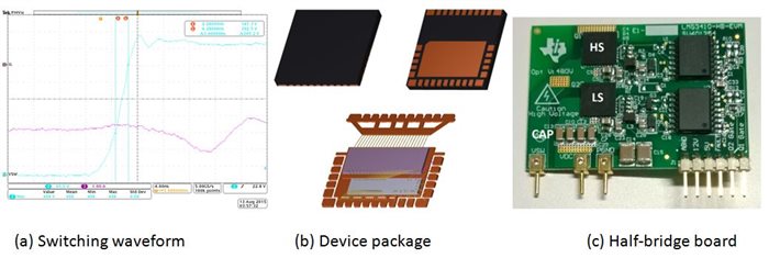
Designed with TI’s latest GaN technology, the power stage’s switch-node waveform shown in Figure 1a, looks truly impressive, from 0V to 480V at a 120V/ns slew rate, with less than 50V overshoot.
 Figure 1 TI’s 600V Half Bridge Power Stage - Switching Waveform (a); Device Package (b); Picture of Half Bridge Board (c).
GaN FETs have low terminal capacitance, and thus enable fast switching. When a GaN half bridge switches at high di/dt, however, the power-loop inductance introduces ringing/overshoot at the high-voltage bus and switch node. This limits how fast the GaN FETs can switch.
Traditional power packages often have high inductance from both leads and bond wires due to long leads and large package sizes. Overshoots as high as a few hundred volts have been observed with leaded packages. The key to reducing overshoot is to minimize the power-loop inductance.
To reduce lead inductance, TI offers its single channel GaN power stage products in surface-mount quad flat no-lead (QFN) packages. As shown in Figure 1b, TI designs the power loops and gate loops to have low inductance internal to the QFN. TI’s GaN half-bridge evaluation module (EVM), shown in Figure 1c places the high and low side devices and bus capacitors close together and returns the power loop at the board layer immediately underneath the devices. This minimizes the size of the power loop, thus keeping the loop inductance low.
TI’s advanced packaging and board design reduces the power-loop inductance to a few nano-Henries. This low-inductance design, integrated with an optimized driver, enables the LMG3410 to switch at slew rates >100V/ns with less than 10% overshoot. With the LMG3410, you can design power converters to switch fast for better efficiency, with low-voltage overshoots and reduced electromagnetic interference (EMI).
TI’s LMG3410 GaN power stage enables power-supply designers to develop higher-density and higher-efficiency power supplies. The device’s ability to reliably switch at high slew rates, combined with an integrated driver with over-current and over-temperature protections, simplifies your job of developing industry-leading power solutions.
Additional Resources:
- Discover more GaN blogs
- Read how to optimize GaN performance with an integrated driver