SSZTAK9 november 2016 ADC32RF45 , LMX2592
Radio frequency (RF) sampling data converters support very wide signal bandwidths and a variety of modulation schemes. The clocking performance for the RF sampling data converter is very important. I previously discussed the importance of the sampling clock and the implications of clock jitter in RF sampling data converters. Now, I want to look more closely at the phase-noise performance of the clock and its implications in real-world systems.
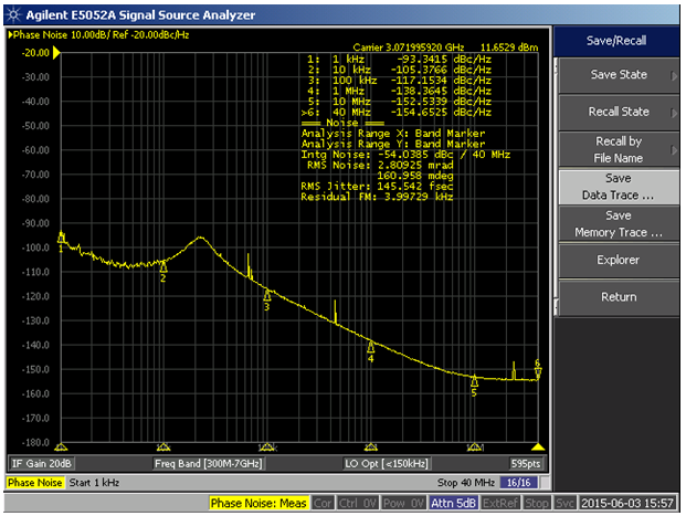
Figure 1 shows an example of a phase-noise plot. Equation 1 defines the total phase noise by integrating the phase noise response over a desired frequency range:

For proper analysis, you must define the frequency limits of integration. What should those limits be? It depends on what you specifically want to measure. For example, if you are interested in the adjacent channel power ratio (ACPR) of a wideband modulated signal, you would integrate across the adjacent frequency band. If you were more interested in the error vector magnitude percentage (EVM%), then you would set the integration limits to the in-band frequency. Or, if your intent is to calculate the signal-to-noise ratio (SNR) of an analog-to-digital converter (ADC), you would set the limits to the smallest capture bin (around a few kilohertz), to the maximum bandwidth of the clock’s input circuit or to the instrument’s maximum bandwidth.
You can use jitter to quantify the data converter’s clock performance. Jitter is a conversion of clock-noise power to the root-mean-square (RMS) movement of the clock-sampling instant in time (measured in seconds). Equation 2 shows the conversion of clock-noise power to jitter:

Let’s look at an example using the phase-noise plot from Figure 1. The limits of integration are set to 1kHz and 40MHz. The latter frequency is the upper limit of the phase-noise analyzer. Since the response has hit the noise floor by this frequency, there is minimal impact by cutting the upper frequency off at this point. The instrument provides a single-sideband (SSB) clock noise within those limits as -54dBc. Applying Equation 2 with a clock frequency of 3GHz, the RMS clock jitter is 145fs. You must add a factor of 2 to convert the SSB measurement to double sideband. Combining this jitter with the aperture jitter of the clock determines the overall jitter. With an RF sampling ADC that has a 70fs aperture jitter, the clock source defined in this example would definitely be the limiting factor.
 Figure 1 Phase-noise Plot
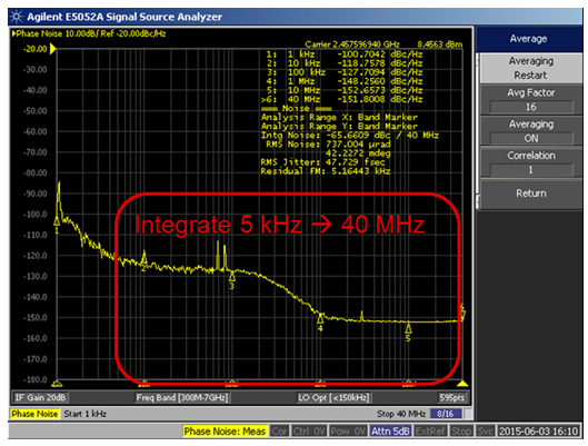
Figure 2 shows the clock phase-noise sweep of a lower phase-noise source. Here, the limits of integration are set to 5kHz (the lowest ADC bin size), to the instrument maximum of 40MHz. The phase noise in this case is -70.6dBc. Applying Equation 2 with a clock frequency of 2.4576GHz yields an RMS jitter of 27fs. When operating with the same 70fs aperture jitter converter, this clock will contribute to overall jitter, but it will not be the dominant factor.
 Figure 2 Low Phase-noise Clock
Source
Figure 2 Low Phase-noise Clock
SourceFor a digital-to-analog converter (DAC), clock jitter’s impact to ACPR is a concern. ACPR is a measure of the power in an adjacent band that may interfere with other users and therefore is strictly controlled. With a 5MHz-wide Long Term Evolution (LTE) carrier, the adjacent channel begins 5MHz away from the fundamental channel and is 4.5MHz wide. Clock-noise power is integrated from 2.75MHz to 7.25MHz to determine the impact to ACPR performance. In most cases, these offsets correspond to the tail end of the response where the performance is at or near the clock’s thermal noise floor. Jitter impact at that level is usually not significant enough to dominate ACPR performance. The DAC’s inherent linearity performance (i.e., the intermodulation distortion) is the limiting factor.
On the other hand, EVM% performance is determined within the band. Here, the limits of integration are set to the first subcarrier, located at around 7kHz to the channel end at 2.25MHz (one sideband). Within this part of the curve, jitter is more significant and will contribute to EVM% performance. There are other factors related to intermodulation and aperture jitter that may be more significant contributors, but the phase-noise performance of the clock plays a part.
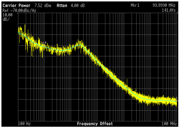
Figure 3 shows the phase-noise plot of the LMX2592 synthesizer operating just under 3GHz. It offers an excellent clock source to the ADC32RF45 RF ADC, sampling up to 3GSPS or for higher-frequency RF DACs (up to 9GSPS). The low integrated phase noise of the phased lock loop (PLL) provides good EVM% performance and low SNR performance. The low spot phase noise of the voltage controlled oscillator (VCO) at 800kHz and beyond impacts ACPR and receiver blocker performance only minimally. This clock solution is offered on the ADC32RF45 evaluation board for easy evaluation.
 Figure 3 Phase-noise Plot of the
LMX2592 at 2.949.12GHz
Figure 3 Phase-noise Plot of the
LMX2592 at 2.949.12GHzRF sampling converters are the high-performance engine to drive your latest designs to larger bandwidths not previously possible. Check out TI’s portfolio of high sampling ADCs above 1 GHz. Just like a high-performance vehicle needs a good set of tires to realize its true performance, these RF sampling converters need a low phase noise clock. Explore TI’s high performance synthesizers capable of getting the best performance out of your converters.
Additional Resources
- Read my other blog on why clocking is so important for RF sampling applications.
- Explore the Clocking Solution Reference Design for GSPS ADCs.
- Watch a training video that provides information about the impact of clock jitter on an ADC’s SNR.
- Learn more about designing with RF sampling data converters from my blog series.