SSZTAK6 november 2016 TPS61253 , TPS61258
The most efficient way to solve a problem with a converter such as failure to startup, output voltage unstable, etc. is to do some basic debugging. Basic debugging would rule out some obvious problems, like fault assembling or the wrong components and, the debugging data can help support engineers of TI to find the root cause quickly. In this blog post, we will talk about tips for debugging a boost converter.
Check the Problem in Another Board
Figure 1 shows the internal diode between the GND pin and the other pins in the IC. You can use a multimeter to test this diode and check for a soldering problem. The multimeter will show approximately 0.7V if the soldering is good. For some special pins, there may be two diodes in series instead of one. In those cases, the multimeter will show 1.4V.
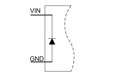 Figure 1 Diode Between VIN and GND
Pin
Figure 1 Diode Between VIN and GND
PinYou can check for IC damage by measuring the resistance between the GND pin and any other pins during power off. The circuits (internal or external) connected to the pins may be damaged if the resistance is much lower than the normal ICs. The damage is mostly caused by voltage overstress, which may result from electrostatic discharge (ESD) because of mistaken handling, bad printed circuit board (PCB) layout or a high voltage out of the IC’s specification from an external source.
Check the Schematic and Components Selection
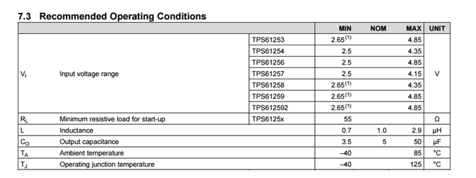 Figure 2 Recommended Operating
Conditions for the TPS61253
Figure 2 Recommended Operating
Conditions for the TPS61253A ceramic capacitor’s effective capacitance is related to its DC bias voltage. For example, the effective capacitance of a 10µF/0603 capacitor, such as the GRM188R60J106ME47 from Murata, is only 3µF at a 5V bias voltage condition. The current flowing through the inductor should be below the saturation current at any condition. Otherwise, the inductance may decrease below the recommended range, which could cause unexpected problems.
Check the Layout
Check the Operating Waveform
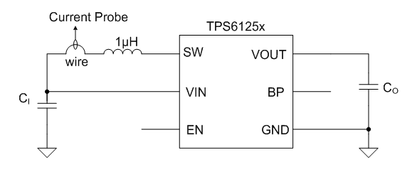 Figure 3 Measuring the Inductor
Current
Figure 3 Measuring the Inductor
CurrentMeasure the four waveforms in the same picture if possible. Figure 4 shows the waveforms of the TPS61258 at light and heavy load conditions. In the waveforms, CH1, CH2, CH3 and CH4 are VOUT, SW, VIN and ICOIL (inductor current), respectively. CH1 is set to DC coupling with a 5V DC offset. So you can easily check both the DC voltage and AC ripple of the TPS61258 output voltage.
At light load conditions, the TPS61258 operates in power-save mode, during which the device switches several cycles and stops for a period of time. At heavy loads, the TPS61258 keeps switching with a 3.5MHz frequency.
During device switching, ICOIL increases linearly when the switch is approximately 0V and decreases linearly when the switch is approximately 5V.
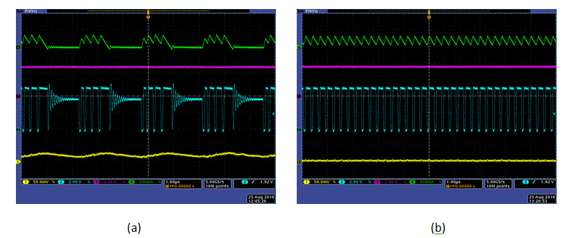 Figure 4 Operating Waveforms of the
TPS61258 (CH1 VOUT, CH2 SW, CH3 VIN, CH4 ICOIL) at Light Load, in Power-save
Mode (a); and at Heavy Load (b)
Figure 4 Operating Waveforms of the
TPS61258 (CH1 VOUT, CH2 SW, CH3 VIN, CH4 ICOIL) at Light Load, in Power-save
Mode (a); and at Heavy Load (b)One device may operate abnormally if its operating waveform is not similar to the waveforms in Figure 4. You can determine the root cause of the problem from the waveform, such as current-limit trigger, device unstable, VIN out of the specification, etc.
Record the Debugging Data and Contact Support
More Suggestions
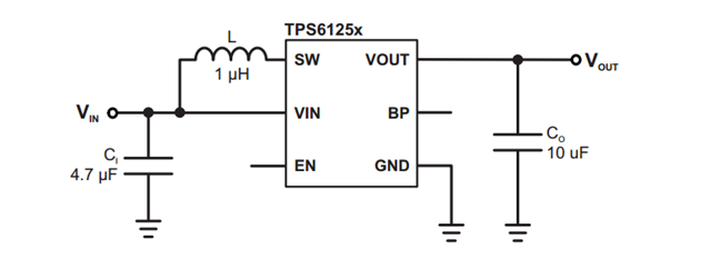 Figure 5 TPS61253 Boost Converter Schematic
The next time you are debugging a boost converter, refer to the tips discussed in this blog for help.
- Confirm the problem in other boards.
- Double-check the schematic and external components.
- Double-check the PCB layout.
- Measure the operating waveforms to observe abnormal behavior.
- If you still haven’t resolved the problem, record the experimental data and ask TI for help on the E2E Community Non-Isolated DC/DC Forum.