SSZTAJ8 december 2016 THS4551
One of my standard interview questions for new college graduates is to describe the non-ideal aspects of an operational amplifier (op amp). While most candidates start with open-loop gain, offset voltage, bandwidth and noise, only a few mention input bias current. Even experienced circuit designers often have questions about input bias current and its effects. In this post, I’ll answer some of these questions and hopefully clear up some misconceptions.
Q: What Is Input Bias Current?
A: The term “input bias current” (IB) in datasheets – for both op amps and fully differential amplifiers (FDAs) – refers to the DC currents flowing into or out of the amplifier’s input pins to create a defined operating point during normal operation, as shown in Figure 1.
 Figure 1 Definition of Input Bias
Current for a Simple PNP Input Stage
Figure 1 Definition of Input Bias
Current for a Simple PNP Input StageBecause a MOSFET requires very little DC gate current to operate, the input bias current of a CMOS amplifier is dominated by leakage from electrostatic discharge (ESD) protection cells and other secondary circuits connected to the inputs. The magnitude of this leakage current is small – on the order of picoamps (pA). Since the inputs of bipolar junction transistor (BJT) amplifiers require base currents for proper bias, however, the BJT input bias current is a lot larger – on the order of microamps (µA). Hence, input bias current is an important issue for BJT amplifiers.
Q: Why Do You Need BJT-input Amplifiers?
A: Since CMOS amplifiers have almost negligible input bias currents, why do you even need BJT amplifiers? The answer is that a BJT has much larger transconductance (gm) compared to a CMOS transistor at the same quiescent current. In addition, matching between BJTs is also a lot better, and so is its flicker (or 1/f noise). All three advantages are crucial for high-speed precision amplifiers; hence, BJT inputs are ubiquitous in high-performance op amps and FDAs.
Q: How Do You Evaluate the Effects of Input Bias Currents?
A: While using amplifiers with significant input bias currents often requires some additional design considerations, you might be surprised to find how little they actually affect system performance. Once you understand the effects of input bias current, you can weigh the benefits of a BJT-input amplifier against these effects.
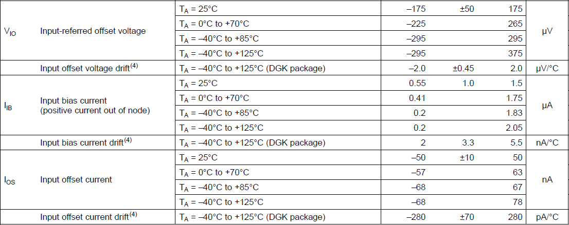
Let’s investigate the effects of input bias currents using the FDA circuit shown in Figure 2. The THS4551 is the newest addition to TI’s family of precision analog-to-digital converter (ADC) drivers. The THS4551 features not only 150MHz bandwidth on 1.35mA Iq, but also ±2µV/°C max VOS drift, as shown in Table 1. The BJT-input architecture enables such performance but creates a notable IB.
 Figure 2 THS4551 FDA Circuit with 1%
Resistors
Figure 2 THS4551 FDA Circuit with 1%
Resistors
|
Focusing on the mathematically simplest case, let’s first assume that the FDAs are always connected with symmetrical feedback elements, since this leads to minimum signal conversion from the common-mode errors to the differential output.
You can calculate the “output referred” offset voltage VOOS in two steps. First, find the amplifier’s positive and negative summing-junction voltages using Equation 1:
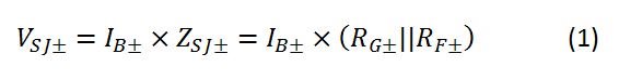
Then, use Equation 2 to calculate VOUT based on the gain from the summing junction to the output, which is the noise gain:

Combining Equations 1 and 2 together, you can calculate VOOS at the output as the difference between these two output voltages with Equation 3:
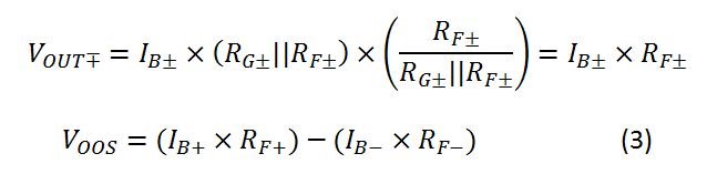
The output VOOS is simply the difference between the input bias currents on each side, multiplied by their respective feedback-resistor values (RF). The gain resistor (RG) has dropped out of the VOOS equation. Intuitively, this is because a small RG, which would have reduced the impact of IB on the summing-junction voltage, also increases the noise gain from summing junction to output, and the two effects cancel each other.
Let’s use the circuit in Figure 2 and the specs of the THS4551 in Table 1 to calculate the worst-case output VOOS from each contributing factor (input VOS, IB and IOS), listed in Table 2.
| Contributing factor | 25°C max error | Worst gain to output | Worst-case contribution to output VOOS (µV) | Gained up by |
|---|---|---|---|---|
| Input VOS | ±175µV | 3.04V/V | ±532 | Noise gain |
| IB± | 1.5µA | ±20Ω | ±30 | Feedback resistor mismatch |
| IOS | ±50nA | 1.01kΩ | ±50.5 | Feedback resistor |
Now, let’s look at four cases for different resistor values and tolerances in the circuit. For two values of RF (1kΩ and 5kΩ) and two tolerances (1% and 0.1%), Table 3 shows the results.
| Case | RF (kΩ) | RF tolerance (%) | Worse-case output VOOS terms (µV) | ||
|---|---|---|---|---|---|
| VOS | IB± | IOS | |||
| 1 | 1 | 1 | ±532 | ±30 | ±50.5 |
| 2 | 1 | 0.1 | ±526 | ±3 | ±50.1 |
| 3 | 5 | 1 | ±532 | ±150 | ±252.5 |
| 4 | 5 | 0.1 | ±526 | ±15 | ±250.3 |
Similarly, Table 4 shows the results for the output-offset drift.
| Case | RF (kΩ) | RF tolerance (%) | Worse-case output VOOS drift terms (µV/°C) | ||
|---|---|---|---|---|---|
| VOS | IB± | IOS | |||
| 1 | 1 | 1 | ±6.1 | ±0.11 | ±0.283 |
| 2 | 1 | 0.1 | ±6 | ±0.01 | ±0.28 |
| 3 | 5 | 1 | ±6.1 | ±0.55 | ±1.41 |
| 4 | 5 | 0.1 | ±6 | ±0.06 | ±1.4 |
A couple of takeaways:
- A well-designed BJT-input FDA or op amp should be able to handle several kilo-ohms of RF without much effect on DC performance.
- When DC performance is a concern, consider improving the resistor RF and RG tolerances to 0.1%, which is a simple and inexpensive method to mitigate the negative effects of IB.
Q: What about Input-current Noise?
A: Most of this post is about the impact of IB and IOS on offset voltage and offset-voltage drift. Another important effect of input current is added noise. Luckily, noise is just a time-varying offset, so you can calculate the effect of noise just as you calculated the effect of offset. For example, the output-voltage noise due to the input-current noise is simply
Another issue worth mentioning is internal input-bias cancellation. Various cancellation techniques can usually reduce IB from the level of microamps to nanoamps. The IOS will also be reduced, although not nearly as much. However, these cancellation techniques usually increase input-current noise due to uncorrelated noise from the cancellation current. So if noise limits your system’s performance, input-bias cancellation is likely not the right choice.
Conclusion
Additional Resources
- Read more about the THS4551 and learn about the equations involving FDA offset calculations.
- Check out this module on input bias current from TI Precision Labs.
- Learn about TI’s entire portfolio of high-speed op amps and explore related technical resources.