SSZTAJ5 december 2016 TPS22915 , TPS22918 , TPS22919 , TPS25924
When a semiconductor lists quick output discharge (QOD) as a feature, it will quickly discharge the output when the device is disabled (or in an “off” state). In other words, when VOUT is disconnected from VIN, VOUT will instead be connected to ground through internal circuitry, preventing the output from “floating” or entering into an undetermined state. Figure 1 shows a simplified block diagram of QOD circuitry.
 Figure 1 Block Diagram of a Load
Switch, with QOD Circuitry in Blue, Showing the Discharge FET, Inverter and
Discharge Path from vOUT To Ground. the Soft-start Capacitor Is Also
Shown in Blue.
Figure 1 Block Diagram of a Load
Switch, with QOD Circuitry in Blue, Showing the Discharge FET, Inverter and
Discharge Path from vOUT To Ground. the Soft-start Capacitor Is Also
Shown in Blue.The main benefit of adding QOD functionality to a system is simple: any power rail on VOUT of a QOD-enabled device will be at a known “zero” or “off” state when the device is disabled. This ensures that when you are designing your system – and especially when you are working out the timing for your power sequencing – that none of your power rails are left floating. Knowing the state of all power rails in your system (and thanks to QOD, knowing that they are actually turned off/grounded), allows you to reduce the number of “variables” in your design, lowering the risk of your design not working as intended.
How to Implement Quick Output Discharge in Your Next Design
 Figure 2 Simplified Block Diagram of the TPS22915, Outlining QOD Circuitry
All load switches with QOD functionality contain an additional FET between the VOUT pin and ground pin (GND), as shown by the dotted outline in Figure 2. This creates a pull-down resistance to quickly discharge VOUT to ground. While some devices, such as the TPS22919 and TPS22918, allow you to place your own discharge resistor, most have an integrated, fixed QOD resistance. As the QOD resistance will vary for each product, you can use Equation 1 to calculate the exact QOD resistance needed for your specific power down sequencing application.
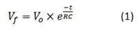
where Vf is the final VOUT voltage; Vo is the initial VOUT voltage; R is the value of the output discharge resistor; and C is the output bulk capacitance on VOUT.
Can you add QOD to a device that does not already integrate this feature? In some cases, you can multiplex certain pins of devices to provide additional functionality. One such example is the BFET pin of the TPS25924 eFuse. This pin normally drives an external blocking FET to protect a system against reverse current, as shown in Figure 3.
 Figure 3 Adding Reverse-current Protection with an External Blocking FET on the TPS25924’S BFET Pin
You can reconfigure this pin to provide QOD functionality even though it is not integrated. This can be accomplished through a very similar circuit, as shown in Figure 3, replacing the blocking FET with a discharge resistor (RDCHG in Figure 4).
 Figure 4 Adding QOD Functionality Using the TPS25924’S BFET Pin
Keep in mind that while QOD is beneficial in most situations, it is not always good to have. In power multiplexing applications, the QOD circuitry would create a constant path to ground on the output of the multiplexer. Additionally, if a supercapacitor is on the output of a power switch, that switch better not have QOD! If it does have QOD, it will drain the supercapacitor’s stored charge, wasting energy. Check out our load switch portfolio, which contains devices both with QOD and without QOD functionality, facilitating any power design.
Additional Resources
- Download the application note, “When to Make the Switch to an Integrated Load Switch.”
- Watch the video, “How and why to replace discrete MOSFETs with load switches.”