SSZTAH4 january 2017 LM53602 , TPS61175
In switching power supplies such as a buck converter, the duty cycle controls the output voltage with respect to the input voltage. While a higher switching frequency is great for reducing the solution size by enabling the use of a small inductor, there is a minimum on-time that must be satisfied in order for the switching power supply to function properly. In other words, the high-side FET must be turned on for a certain amount of time within each switching period such that the condition in Equation 1 is met:
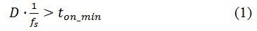
where D is the duty cycle and fs is the switching frequency.
Several factors within the circuit necessitate this minimum on-time. For example, one factor is the current spike on the leading edge of the current waveform in the high-side FET. Since the FET has parasitic gate capacitances Cgs and Cgd, and the current through the high-side FET changes abruptly when it turns on, the capacitances behave similarly to a short in the presence of the changing current. This results in a current spike. In order to prevent this from triggering the current limit, current-limit violations are ignored during blanking time (tLEB in Figure 1). Therefore, the minimum on-time of the switching circuit must be larger than the blanking time – otherwise, the current-limit protection will be turned off for longer than the actual on-time.
 Figure 1 Current Spike on the Leading
Edge of the Current Waveform of the High-side FET
Figure 1 Current Spike on the Leading
Edge of the Current Waveform of the High-side FETOther factors include the rise and fall time of the switch-node voltage and level-shifter delay to set the gate voltage on the high-side FET.
Devices will behave differently when the on-time falls to its minimum, sometimes resulting in problems that may seem unexpected. For example, the switching power supply may start pulse skipping (shown in Figure 2) as a way to compensate for the inability to further decrease the on-time while still maintaining the output voltage. This results in a larger output voltage ripple and unknown harmonics from changes in switching frequencies.
 Figure 2 Pulse-skipping Waveform in the
TPS61175 Boost Converter
Figure 2 Pulse-skipping Waveform in the
TPS61175 Boost ConverterOther devices may instead use frequency foldback to allow the duty cycle to decrease. In this case, the switching frequency drops but the pulses occur regularly – unlike in pulse skipping where entire pulses are dropped. Figure 3 shows an example of this functional mode.
 Figure 3 Frequency Foldback in the
LM53602 at vOUT = 5V
Figure 3 Frequency Foldback in the
LM53602 at vOUT = 5VIt is critical to note these issues when choosing a device to use for your switching power-supply needs. For example, in automotive applications, frequencies within any circuit must not fall within the AM band. Otherwise, they may interfere with the radio signal and clobber any information that was sent via that frequency band. Any application that involves information transfer on a certain frequency band must pay special attention to the possibility of interference from the regulator. Designs that use devices with a smaller minimum on-time will therefore encounter fewer complications.
One example of a great device with a small minimum on-time is the LM53602 buck converter. Its minimum on-time of 50ns enables a larger range of possible duty cycle and frequency pairings. As long as switching power-supply designers are cognizant of the significance of minimum on-time, their designs will be able to work more effectively in a larger variety of situations.