SSZTA99 april 2017 TPS548D21
With the emergence of Internet of Things (IOT) applications, more and more application-specific integrated circuits (ASICs) and field-programmable gate arrays (FPGAs) are being deployed into cloud computing and server system applications. These high-performance end applications demand higher processing power and ever-increasing clock speeds.
Voltage and power-scaling technologies have enabled very powerful and versatile power-management systems on smaller and denser integrated circuits, significantly reducing power losses and optimizing device junction temperatures while fulfilling the high-performance requirements of the system. Adaptive voltage-scaling optimization (AVSO) is one of the voltage scaling implementations.
There are different methods to AVSO implementations, either via digital and/or analog means. The most common are through PMBus or the I2C interface. You can program the initial supply voltage to power up the ASICs, FPGAs or a microprocessor with reasonable accuracy. Once the processor completes the boot-up sequence, it communicates with a voltage regulator, either via a PMBus or I2C command set. The purpose of this communication is to tell the regulator to adjust the output-voltage level based on the performance demand of the host. The most popular standard commands are VOUT_COMMAND and VOUT_MARGIN. In order to facilitate such dialogs, both the host and voltage regulator need to implement the same digital communication protocol.
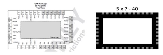
Sometimes a digital implementation is just not a viable option due to the lack of hardware, software or firmware in the end system. In systems where there is still a need to optimize power dissipation, consider an analog voltage regulator employing the use of a reference input (REFIN). One such example is TI’s TPS548D21 (see Figure 1) - a fully integrated 40A high-performance synchronous step-down converter supporting AVSO and full differential sensing in a compact 5mm-by-7mm stacked-clip quad flat no-lead (QFN) package.
 Figure 1 TPS548D21 Pin Out Diagram and
Bottoms up View of Package
Figure 1 TPS548D21 Pin Out Diagram and
Bottoms up View of PackageManaging voltage scaling and sequencing is very easy using the TPS548D21. The TPS548D21 device can operate in either tracking (voltage scaling) or sequencing mode through MODE pin-strap configurations.
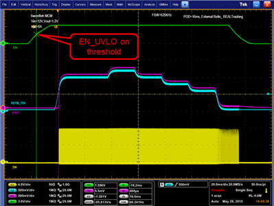
For voltage scaling/tracking, the reference tracking input (REFIN_TRK) allows an external reference voltage source to set the reference voltage of the TPS548D21 device (Figure 2). This voltage source can be anywhere between 0V to 1.25V, although its input impedance must be much less than 100kW. When the external voltage source transitions up and down between any two voltage levels (between 0.5V to 1.25V), the slew rate must be controlled to no more than 1mV/µsec. A tracking accuracy of less than 1% is possible between 0.5V to 1.25V.
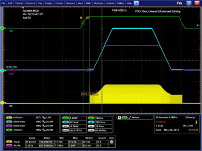
The external sequencing feature of the TPS548D21 device allows ratiometric sequencing of multiple converters during startup and shut down by applying the same voltage source on the REFIN_TRK pin of the TPS548D21 (Figure 3). When programming the TPS548D21 device to perform external tracking (sequencing), the REFIN_TRK voltage must start from 0V and the external applied ramp must ramp upon completion of the power-on delay. The ramp time must also be longer than 1ms in duration.
 Figure 2 Tracking Waveform
 Figure 3 Sequencing Waveform
An additional benefit of analog tracking is the on-the-fly change resulting in no latency time between reference input and output response, resulting in improved system response and reduced power loss.
The next time you are powering an ASIC or FPGA consider a full analog approach to managing voltage scaling and sequencing. See the TPS548D21 data sheet and get started now.