SSZTA52 may 2017 TPS53315 , TPS53319
PRODUCTION DATA
Many synchronous buck converter designers face a common issue: how best to connect the open drain power-good flag, also known as the power-good (PGOOD) pin. In this post, I will explore the expected behavior of power good when it is tied to various different pull-up sources. There has been some misinformation floating around that hopefully this post will clarify.
As many converter data sheets describe, the function of the PGOOD pin is to indicate high after the switcher output gets within the target regulation. For instance, when the output voltage of one of TI’s step-down regulators with integrated switchers is within +10% and -5% of the target value, internal comparators detect a power-good state and the open-drain field-effect transistor (FET) turns off, enabling the power-good signal to rise to the pull-up voltage. If the output voltage goes outside of +15% or -10% of the target value, the open-drain FET turns on and the power-good signal becomes low after a short 2ms delay. Power good will also go low (regardless of output voltage) in a few other scenarios, such as when enable goes low, in order to facilitate quick shutdown sequencing in daisy-chained systems.
The recommended pull-up for the PGOOD pin is to tie it to the internally generated VREG pin or BP pin. The output remains low when the device is disabled or not powered, which has the benefit of defining the power-good state before any bias is present. Some users with different input/output (I/O) voltages prefer to pull the PGOOD pin up to an external bias like 3.3V, which can introduce some complications due to timing. Before providing VIN/VDD (typically 12V), there is nothing powering the comparators and logic “defining” the power-good state. At this time (before applying power), the open-drain FET’s gate voltage is determined by leakages and is more likely to turn off than to turn on. Coupling that fact with an external pull-up voltage that could be present before VIN/VDD can lead to the PGOOD pin showing high during an otherwise PBAD state.
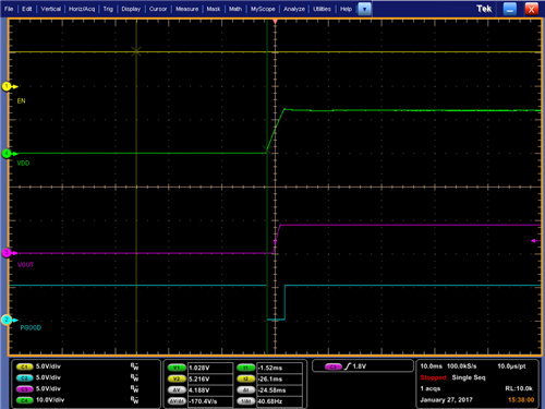
Figure 1 through Figure 5 are scope shots of PGOOD pulled up by VREG, and PGOOD pulled up by an external voltage using the TPS53315 and TPS53319 synchronous buck converters. Note how PGOOD will float up to the pull-up voltage, even though the device is not regulating.
 Figure 1 The TPS53315 Power Good Is
Clean with No Glitches
 Figure 2 The TPS53319 Power Good Is
Clean with No Glitches
 Figure 3 The TPS53315 Power-good Glitch
That Results in PGOOD Ties to Enable: Enable Power Goes High First, Then
VDD
 Figure 4 The TPS53319 Power-good Glitch
That Results in PGOOD Ties to Enable: Enable Power Goes High First, Then
VDD
 Figure 5 The TPS53319 Power-good Glitch
That Results in an External 3.3V Pull-up on PGOOD Being Present before
VDD/VIN
Figure 5 The TPS53319 Power-good Glitch
That Results in an External 3.3V Pull-up on PGOOD Being Present before
VDD/VINIt is best to use a self-derived voltage through dividers in order to guarantee the logic state of the PGOOD pin at all times. When using external always-on voltages, the downstream logic needs extra consideration in order to avoid a small power good glitch before the controller power supply (VDD) gets up to ~1V. Get more information on all of TI’s buck converters with power good.