SSZT950 september 2017 TPS732
A low-dropout (LDO) regulator’s nature is to regulate a voltage by turning excess power into heat, making this integrated circuit an ideal solution for low power, or small VIN to VOUT differential applications. With this in mind, choosing the right LDO with the right package is crucial to maximizing an application’s performance. This is where some designers have nightmares, since the smallest available package isn’t always a perfect fit for the desired application.
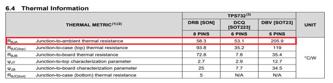
One of the most important features to consider when selecting an LDO is its thermal resistance (RθJA). This feature illustrates how efficient the LDO is at dissipating heat in a specific package. Higher RθJA values indicate that a package is not very effective at transferring heat, whereas lower values indicate that the device transfers heat more effectively.
RθJA will typically be higher for smaller packages. For example, the TPS732 has different thermal resistance values depending on its package: the small-outline transistor SOT-23 (2.9mm by 1.6mm) package thermal resistance is 205.9°C/W, compared to the SOT-223 (6.5mm by 3.5mm) package’s 53.1°C/W. This means that the TPS732 will experience a rise of 205.9°C or a 53.1°C per 1W dissipated. You can find these values on the device’s data sheet under Thermal Information as shown in Table 1.
|
Do You Have the Right Package?
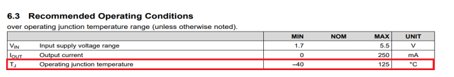
The recommended operating junction temperature of an LDO is anywhere between -40°C to 125°C; again, you can check these values on their respective data sheets, as shown in Table 2.
|
What these recommended temperatures mean is that the device will operate as stated in the Electrical Characteristics table of the datasheet. You can use Figure 1 to determine which package will operate at the right temperature:
 Figure 1 Junction Temperature
Equation
Figure 1 Junction Temperature
EquationWhere TJ is the junction temperature,
TA is the ambient temperature,
RθJA is the thermal resistance (from the data sheet),
PD is the power dissipation and
Iground is the ground current (from the data sheet).
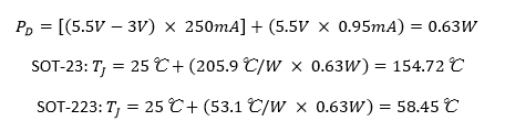
Here is a quick example using the TPS732 to regulate 5.5V down to 3V, supplying 250mA and using both the SOT-23 and the SOT-223 package.
Thermal Shutdown
A device with a junction temperature of 154.72°C not only exceeds the recommended temperature specifications, but it also gets really close to the thermal shutdown temperature. The shutdown temperature is typically at 160°C; this means that if a device’s junction temperature is greater than 160°C then the device’s internal thermal protection circuit is activated. This thermal protection circuit disables the output circuitry allowing the device to cool and protect it from overheating damage. When the device’s junction temperature cools to around 140°C the thermal protection circuit is disabled and re-enables the output circuitry again. If you don’t reduce the ambient temperature and/or the dissipated power, then the device can potentially oscillate on and off as a result of the thermal protection circuit. If you can’t reduce the ambient temperature and/or dissipated power, you’ll have to make design changes to achieve proper performance.
One clear design solution is to use the bigger package, since it operates at the recommended temperature.
Here are some tips and tricks to minimize heat.
Increasing Ground, vIN And vOUT Contact Planes
When power dissipates, heat escapes the LDO through the thermal pad; therefore, increasing the size of the input, output and ground planes in the printed circuit board (PCB) will decrease the thermal resistance. As shown below in Figure 2, the ground plane is usually as large as possible and covers most of the PCB area not occupied by other circuit traces. This sizing guideline is due to the returning current from many components and to ensure that those components are at the same reference potential. Ultimately the contact planes help avoid voltage drops that can hurt the system. A large plane will also help increase heat-sinking ability and minimize the trace resistance. Increasing copper-trace size and improving the thermal interface significantly improves the conduction cooling efficiency.
 Figure 2 PCB Layout of SOT-23 Package
When designing a multilayer PCB, it’s usually a good idea to use a separate layer covering the entire board with a ground plane. This helps you ground any component without the need for additional traces. The component leads connect directly through a hole in the board to the layer containing the ground plane.
Mounting a Heatsink
Heatsinks decrease RθJA, but add size and cost to the system. When selecting a heatsink, the base plate should be similar in size to the device to which it attaches. This will help evenly distribute heat over the heatsink surface. If the heatsink size is not similar in size to the surface to which it attaches, the thermal resistance will increase.
Due to their physical size, packages like the SC-70 (2mm by 1.25mm) and the SOT-23 (2.9mm by 1.6mm) are not often used with a heatsink. One the other hand, you can pair packages like the TO-220 (10.16mm by 8.7mm) and the TO-263 (10.16mm by 9.85mm) with a heatsink. Figure 3 below shows the difference between the four packages.
 Figure 3 Package Differences
You can place a resistor in series with the input voltage in order to share some of the dissipated power, an example of this is shown below in Figure 4. The goal of this technique is to use the resistor to drop the input voltage to the lowest input voltage possible.
 Figure 4 Resistor in a Series
Configuration
Figure 4 Resistor in a Series
ConfigurationSince the LDO needs to stay in the saturation region to regulate properly, you can obtain the minimum input voltage by adding the desired output voltage plus the voltage dropout. Figure 1 expresses the setting of these two LDO properties:
 Figure 5 Maximum Resistance
Equation
Figure 5 Maximum Resistance
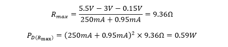
EquationUsing the conditions in the TPS732 example (regulating 5.5V to 3V using 250mA), you can use Figure 1 below to calculate the maximum value of the resistor and the maximum power it can dissipate:
 Figure 6 Maximum Power Dissipated
Equation
Figure 6 Maximum Power Dissipated
EquationMake sure to select a resistor so as not to exceed its “Dissipating Power Rating”. The rating indicates how many watts the resistor can turn into heat without damaging itself.
So if VIN = 5.5V,
VOUT = 3V,
VDROPOUT = 0.15V (from the datasheet),
IOUT = 250mA and
IGROUND = 0.95mA (from the datasheet), then:
Placement
Other heat-generating devices on the PCB can potentially affect the LDO’s temperature if they are within close proximity to the LDO. To avoid temperature increases, make sure to place the LDO as far as possible from those heat-generating devices.
Conclusion
There are many ways to execute an efficient, size-conscious and low-cost thermal solution for an application. The key lies in early design considerations in order to have all options available. Selecting the proper components is not an easy task when managing thermal considerations, but the right devices and techniques will facilitate a successful design process.
Additional resource:
- Check out the Low dropout regulators selection guide.