SSZT917 october 2017 BQ25898
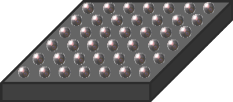
Wafer chip-scale packages (WCSPs) are becoming more popular in portable electronics due to their smaller footprint, lighter weight, better electrical parameters and lower manufacturing costs. WCSPs enable a direct interconnection between the silicon chip and the printed circuit board (PCB). Their minimal footprint frees up a lot of space on the PCB for other components. Figure 1 illustrates a WCSP.
 Figure 1 WCSP Illustration
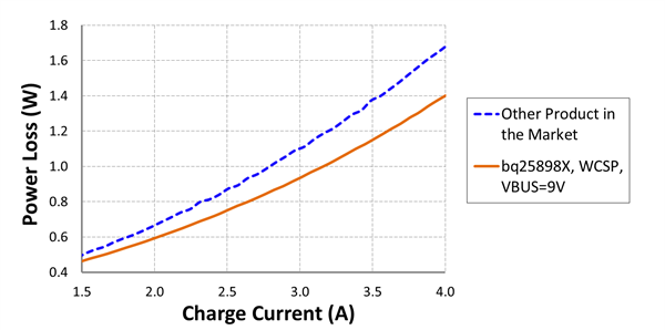
A WCSP also reduces parasitic resistance, inductance and weight by eliminating the extra bond wires, lead frames and encapsulation found in other packages. The lowered resistance in the power-conversion integrated circuit (IC) results in higher efficiency. As Figure 2 shows, the power loss is lower in bq25898x WCSP than in a competing IC family, while also providing 13% more charging current for the same 1W power-loss budget. This is very significant for maintaining the same equipment case temperature at a higher charging current, as discussed in the blog post, “How 1.2% more efficiency can help you charge faster and cooler.”
 Figure 2 Power Loss of bq25898 in WCSP
For the same power loss, however, the IC temperature increase is usually higher in WCSPs due to their higher junction-to-ambient thermal resistance (RθJA). The smaller footprint also leaves little room for component placement and wire routing. Optimizing PCB layout and maintaining good thermal performance are therefore big challenges.
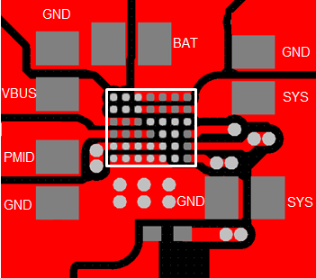
Figure 3a is an example layout of the bq25898. All critical components, input (PMID and VBUS), system (SYS) and battery (BAT) capacitors are placed next to the device pins, keeping the high-frequency current loop at a minimum. All power lines use the maximum copper pours; almost the entire PCB is covered by copper. A big ground copper pour is created at device GND, and well connected to other GNDs.
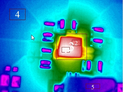
Figure 3b is a thermal image of the bq25898 taken at 3A Charging current with a 9V input and a 3.9V battery . As you can see, heat is evenly distributed across the IC, with no excessive heat buildup or hot spots.
This experiment shows that a PCB layout like that shown in Figure 3 can reduce the IC temperature from 55°C to 52°C compared to a “normally” laid-out PCB. For more details about layout optimization, see the application note, “Achieving the Optimal Thermal Performance for Chip Scale Package.”
(a)

(b)
 Figure 3 PCB Top-layer Layout (a); and Thermal Image (b)
As you can see, it’s possible to highly enhance thermal performance with an optimized PCB layout to avoid hot spots. If done properly, WCSPs provide a lighter, faster and cooler charger, with a better customer experience.
Additional Resources:
- Read the application note: Achieving the Optimal Thermal Performance for Chip Scale Package