SSZT689 june 2018 SN65HVD82 , THVD1550
The RS-485 interface is widely used in industrial applications because of its robustness and long-distance communication capability. Since the RS-485 standard was first introduced to the market in 1998, electronic systems have increased in size and complexity. Many end equipments, such as motor drives, PLCs, and industrial PCs, now require high-speed (>10Mbps) communication. TI’s THVD1550 is the latest TI RS-485 transceiver that can support data rates as high as 50Mbps. In this post, I’ll show you how to evaluate the THVD1550’s power dissipation with such high-speed transmissions. By doing so, you can understand how the power is consumed and evaluate the system’s thermal performance.
To calculate the power dissipation, you can divide the power into several parts. After successfully evaluating each portion, you put all of them together to obtain the total power. When the device powers on with no external load, the power consumption is used for the integrated circuit (IC) itself. If you add loads at the output pins, the power of driving the load will be drawn from the device. Since RS-485 has differential signaling, the load is usually added between the A and B pins.
Looking further into the loads, you can divide them into two types: resistive and capacitive. The resistive load itself consumes some power, while the capacitive load only transfers the energy between its plates and is not associated with any energy loss. Due to the characteristic of each type, the power calculation is different.
Figure 1 is a diagram of three types of power dissipation.
 Figure 1 The Current Flow of a Typical
RS-485 Transceiver
Figure 1 The Current Flow of a Typical
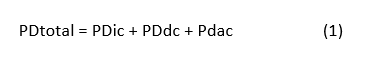
RS-485 TransceiverPDic (blue) is the power the device consumes itself. PDdc (red) is the power from the resistive load and PDac (green) is the power from the capacitive load. The total power is the sum of all these three parts using Equation 1.
To calculate PDic, you can use the value of quiescent supply current, Icc, in the data sheet. It’s 700µA typical in the THVD1550. (In this post, I’ll use typical values; for example, Vcc is 5V.) With the voltage and current values, the device power can be calculated using Equation 2.

If you put a resistive load on the bus, the driver generates a voltage (Vod) on it. The RS-485 standard requires a minimum 1.5V Vod on a 54Ω resistance. In a typical case, 2.7V is generated on 54Ω from the THVD1550’s driver, which means that 50mA current is drawn out of the device.
What’s important here is that you need to distinguish the power dissipation from the load and the power from the device. You only care about the latter for the device’s thermal performance. Therefore, Equation 3 deducts the load power (I2*R) from the total power of the supply (Vcc*I):

Now, let’s look at the switching power – the power needed to drive the capacitive load. To make the calculation easier, split the differential capacitor into two grounded single-ended capacitors (Figure 2).
 Figure 2 Equivalent Capacitive Loading
of a Typical RS-485 Transceiver
Figure 2 Equivalent Capacitive Loading
of a Typical RS-485 TransceiverThe signal on each capacitor has the amplitude of Vod and the frequency of half the data rate (Figure 3). Although the voltages are differentially opposite on the A and B pins, they both consume the same amount of power.
 Figure 3 The Signaling of Output Pins
of an RS-485 Transceiver
Figure 3 The Signaling of Output Pins
of an RS-485 TransceiverHere, you also take the device’s parasitic capacitor into account. In some data sheets, it is called Cod. Let’s take the typical value of 8pF from the SN65HVD82. Assume 50pF load capacitance. Now, the value of each capacitor C in Figure 2 equals the sum of 50pF + 8pF. The switching power is related to the frequency and amplitude. During each charge, the energy consumed from the supply is equal to Equation 4:
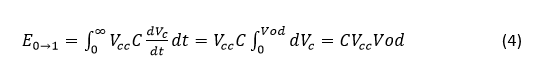
where Vc is the voltage on the capacitor.
At each moment, the instantaneous current flowing on the capacitor is . You integrate instantaneous power over time to get the energy needed to charge the capacitor. Therefore, Equation 5 calculates the power from driving the capactitive load:

After obtaining the value of all three power-dissipation portions, Equation 6 shows that the total value is:

In section 7.5 of the data sheet of the THVD1550, the table shows the test data of the device’s power dissipation, with a 5.5V supply and 125°C temperature at a 50Mbps data rate, which is kind of a worst-case scenario. The values include some nonideal factors like shoot-through current; therefore, you can use them to evaluate the maximum power dissipation of the device in a system design.
Additional Resources
- Read the application report, “AN-805 Calculating Power Dissipation for Differential Line Drivers.”