SSZT674 June 2018 TRS3232E , TRS3243E , TRS3318E , TRS3386E
Other Parts Discussed in Post: TRS3232E
The RS-232 interface is popular in single-ended low-speed serial communications. The interface was originally designed to connect the serial port of a computer to peripheral devices. The Electronics Industry Alliance (EIA)-232 levels are defined as up to ±15V into a 5kΩ load. Thus, RS-232 transceivers need three supplies from the system. Due to the limited on-board supply, single-supply RS-232 integrated circuits (ICs) have been available since the 1980s. These transceivers integrate charge-pump circuitry to generate the required positive and negative voltage levels internally on the IC. The charge pumps need external capacitors to store and transfer the energy. In this post, I’ll explain how the charge-pump circuitry works and how the output voltage is regulated based on it.
How Charge-pump Circuitry Works
Figure 1 is a diagram of the charge-pump circuitry. An internal oscillator generates a clock signal, which is used to control the switches (SW1, SW2, SW3 and SW4).
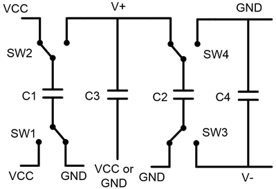 Figure 1 Charge-pump Circuitry Diagram
For illustration purposes, let’s focus on the V+ voltage first. The mechanism of generating the V- voltage is similar. With the internal clock, the voltage will charge on C1 and C3 alternatively (in some literature C1 is called flying capacitor and C3 is called storage capacitor). In the first cycle, C1 charges to VCC (Figure 2).
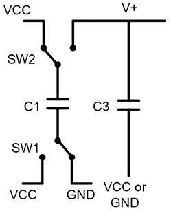 Figure 2 The Diagram of Generating v+ Voltage (Cycle One)
In the next cycle, one end of C1 connects to VCC and the other end to V+ (Figure 3). Since the voltage difference on C1 cannot be changed instantly, V+ becomes two times VCC, with one from the SW1 and the other from the existing charge of C1. Here you assume no loss in the circuitry.
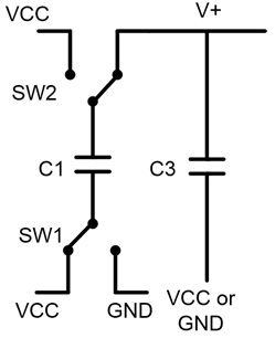 Figure 3 The Diagram of Generating v+ Voltage (Cycle Two)
In the same manner, V- is generated in cycles (refer back to Figure 1). In one cycle, C2 charges to V+. In the next cycle, the charge dumps to V- with the polarity reversed. Therefore, V- maintains the same amount of V+ voltage level but below ground.
How Regulation Works
With charge-pump circuitry, V+ becomes 2Vcc and V- becomes -2Vcc. As long as the clock keeps running, the charging keeps happening. To make the device have better efficiency and produce a better regulated output voltage, a regulator circuitry monitors the output voltage with a feedback loop to control the charge pump (Figure 4).
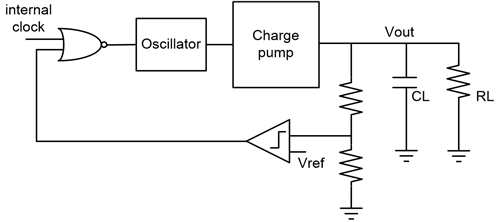 Figure 4 The Regulator Circuitry
Diagram
Figure 4 The Regulator Circuitry
DiagramIf the V+ voltage is higher than a pre-set positive threshold, or V- is lower than a negative threshold, the charge pump stops working. As one of the voltages drops beyond its threshold, the charge pump starts pumping again. Due to this regulation, some ripples are shown on the V+ voltage (Figure 5).
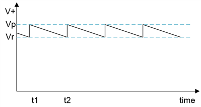 Figure 5 V+ Waveform
Let’s analyze the amplitude of the ripples. Assume the ends of C3 connect to V+ and Vcc (Figure 2). Look at the moment just before time t1 (Figure 4), where the V+ voltage is higher than Vr (threshold) and the charge pump is not yet turned on. V+ droops down by discharging C3. At t1, the voltage decreases to Vr; therefore V+ is equal to Vr. The charge pump starts working and transfers the charge stored on C1 to C3. Without any loss, the charge should be equal in two states. Before the charge transfer, the voltage on C3 is Vr-Vcc and Vcc on C1. After the transfer, both C1 and C3 share the same voltage potential Vp-Vcc. The total charge before and after the transfer is calculated in Equation 1.
Thus, Vp is calculated by Equation 2 with all known values:
Assuming Vr = 5.5V, Vcc = 3.3V and C1 = C3, Vp is 6.05V.
I have several comments about these equations. First, if you assume C1 = C3, the charge can be considered distributed equally between C1 and C3. Therefore. the peak voltage Vp is halfway of Vr (5.5V) and 2Vcc (6.6V). Also, from the equations you can see that from the ripple’s point of view, what matters is not the absolute values of C1 and C3 but the ratio of C1 to C3. In some applications, C3 connects to GND instead of Vcc. In this case, charge Equation 1 becomes Vr*C3+Vcc*C1 = (Vp-Vcc)*C1+V+*C3, resulting in the same Vp.
Similarly, you can calculate the ripple voltage of the V- pin. Equation 3 calculates the peak voltage of V- as:
To make the variables consistent, Vr and Vp are the threshold voltage and peak voltage of V+ used in Equations 1 and 2. Replacing them with the values from the previous calculation and again assuming C2 = C4 results in Equation 4:
The V- voltage shows less amplitude of ripple than V+, since the charge is filtered one more time by external capacitors.
The voltage on the capacitors goes above Vcc with regulation and could become 2Vcc without regulation. Therefore, to play it safe, choose MLCC (X5r or X7r) capacitors with a voltage rating of at least 10V or even 16V.
The Impact of Variable Capacitor Values
Now that you understand how the charge pump and regulator circuitry work, you can play with the external capacitor value to see the impact on the output waveform. The rule of thumb is that if C3 is bigger than C1, then less charge will be dumped to C3. Therefore, less ripples will show in the V+ waveform.
Figure 6 through Figure 8 are some V+ waveforms of various capacitor values from bench testing.
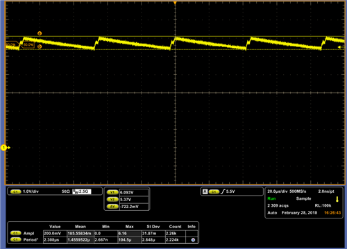 Figure 6 V+ Waveform, C1 = 0.47µF,
C3 = 0.1µF
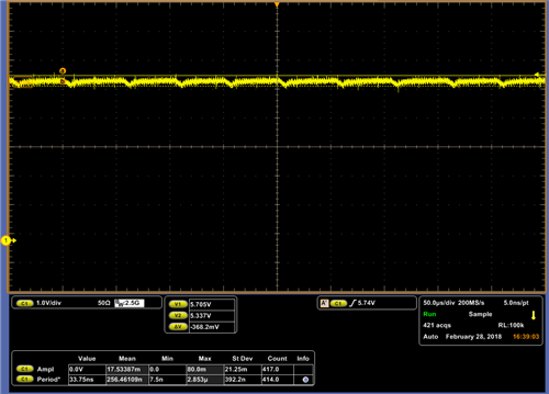 Figure 8 V+ Waveform, C1 = 0.01µF,
C3 = 0.1µF
 Figure 7 V+ Waveform, C1 = 0.1µF,
C3 = 0.1µF
Figure 7 V+ Waveform, C1 = 0.1µF,
C3 = 0.1µFIn these room-temperature tests of TI’s TRS3232E RS-232 line transceivers, the supply is 3.3V. The C3 value remains 0.1µF and C1 value varies from 0.01µF to 0.47µF. Figure 6 shows the highest ripples, with C1 = 0.47µF, and Figure 8 shows the lowest ripples, with C1 = 0.01µF. Be aware that the regulation cycles vary with the amplitude of the ripple as well. Assume that the discharge happens at the same rate on C3. Higher ripples take longer to discharge (44µs in Figure 6), while low ripples have a higher frequency (36µs in Figure 7). The cycle of Figure 8 is mainly governed by the charging time rather than the discharging time. In an additional testing, Figure 9 shows the case when C1 and C3 have the same ratio but with a different absolute value 0.47µF. Comparing Figure 9 with Figure 7, the amplitude of the ripples is close and the frequency is higher (20µs) due to the faster charging and discharging capability of larger capacitors.
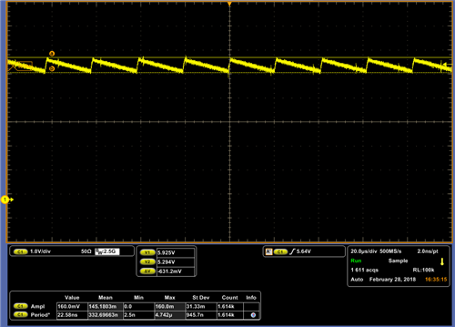 Figure 9 V+ Waveform, C1 = 0.47µF, C3 = 0.47µF
Please be aware in the testing above, the device was running with no load. If a current load is added such as a resistor (RL in Figure 4), the calculation would be different and in general the output voltage would be lower.
Additional Resources
- Read the application report, Design for a Discrete Charge Pump.