SSZT626 september 2018 LM5122 , LMV431
Although a cycle-by-cycle current-limit function exists in most synchronous boost controllers, sometimes engineers will add output overvoltage protection (OVP) in case of emergency to protect discrete circuits. In this blog post, I’ll show you how to achieve accurate output OVP at a very low cost. Although I’ll use the LM5122 synchronous boost controller and its evaluation module (EVM) as an example, the proposed circuits are applicable to other synchronous boost controllers.
The LM5122 multiphase synchronous boost controller is intended for high-efficiency synchronous boost regulator applications. Its control method is based on peak-current-mode control, which provides inherent line feed forward, cycle-by-cycle current limits and easy loop compensation. Figure 1 shows the simplified LM5122 application diagram. Although the cycle-by-cycle current limit function exists, the LM5122 doesn’t provide OVP itself. However, by adding a simple circuit you can achieve accurate-enough output over voltage protection.
 Figure 1 Simplified LM5122 Application
Diagram
Figure 1 Simplified LM5122 Application
DiagramFigure 2 shows a primitive output OVP circuit where the output voltage sense resistor divider consists of R1 and R2. Assuming that Vz is the breakdown voltage of the Zener diode, Vbe is the voltage that falls between the base and emitter of the n-channel p-channel n-channel (NPN) transistor. You can use Equations 1 and 2 to trigger the circuit to run into protection:
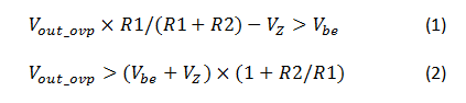
Because Vz and Vbe normally have tolerance and they also vary over temperature, the OVP threshold will vary widely.
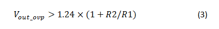
Figure 3 shows another output OVP circuit, which will have more controlled OVP threshold. Again, the output voltage sense resistor divider consists of R1 and R2. The LMV431 is a low-voltage (1.24V) shunt regulator. By comparing the central point of the sense resistor divider and the internal reference pin of the LMV431, OVP will trigger if the central point voltage of the sense resistor divider is higher than the 1.24V reference, as expressed in Equation 3:
Because the LMV431 has an initial small tolerance of 1.5% over temperature, this circuit has more OVP precision than the primitive output OVP circuit with the Zener diode. If the central point voltage of the sense resistor divider is higher than 1.24V, the cathode voltage of the LMV431 decreases, which will cause the base of the MMBT2222 to be high. The collector of the MMTB2222 connects to the undervoltage lockout (UVLO) pin of the LM5122 and the UVLO pin pulls down to 0V. The boost converter enters shutdown mode and stops transferring energy to the output.
 Figure 2 Primitive Output
OVP
Figure 2 Primitive Output
OVP Figure 3 Output OVP Circuit
Using the LM5122 EVM, the OVP voltage is set to 23.5V. In order to verify the OVP circuit, you can adjust the EVM to set the nominal VO as 19.5V, with an additional 10kΩ resistor added to the VO sensing divider. Figure 4 shows the experimental result. LO is the low-side N-channel MOSFET gate drive output. When VO increases to 23.5V after adding the 10kΩ resistor in parallel, the UVLO pulls down to zero and the LM5122 goes into shutdown mode, with all functions disabled.
 Figure 4 Low-side MOSFET Stops
Switching When OVP Triggers
Figure 4 Low-side MOSFET Stops
Switching When OVP TriggersThe reason that you need to use two MMBT2222 and MMBT2907 transistors is because the LM5122 UVLO threshold is 1.2V. The minimum voltage of the LMV431 cathode is above 1.24V. Adding these two transistors will cause the UVLO pin under 1.2V to stop switching.
Figure 5 shows another simplified output OVP circuit without two transistors. The LM5122 controller features a UVLO function, with an external UVLO setpoint voltage divider from the supply voltage VIN to the analog ground pin (AGND). The LM5122 evaluation module has a startup voltage of 8.7V and VHYS is set to 0.5V. The standard value of RUV2 is 49.9kΩ and the standard value of RUV1 is 8.06kΩ. By splitting RUV2 into two resistors RUV2_1, RUV2_2 and connecting the cathode of the LMV431 to the central points of these two resistors RUV2_1, RUV2_2, you can achieve the similar output OVP feature with circuit shown in Figure 3.
 Figure 5 Simplified Output OVP
Circuit
Figure 5 Simplified Output OVP
CircuitFigure 6 shows the experimental result of the second output OVP circuit. When VO increases to 23.5V, the cathode voltage of the LMV431 decreases to 1.24V and the UVLO pin voltage becomes 0.53V. The LM5122 enters standby mode and stops switching. The soft-start capacitor discharges to 0V and after a 5.9ms soft-start time, the device starts switching again. The second output OVP circuit triggers standby mode and is cheaper than the first OVP circuit.
 Figure 6 Low-side MOSFET Stops
Switching When OVP Triggers
Figure 6 Low-side MOSFET Stops
Switching When OVP Triggers