SSZT602 october 2018 LMV431 , TPL0102-100
As smartphones continue to get smarter and larger, battery capacitance is also increasing. Being able to quickly charge a battery is a crucial aspect to consider in power delivery. The rise in popularity of USB Type-C™ with USB Power Delivery (PD) and its programmable power supply (PPS) function lowers charge time by maximizing efficiency in the power adapter and minimizing charging losses on the phone end. PPS allows the adapter to have a variable output voltage by communicating with the device being charged, optimizing charging conditions.
The isolated flyback power-supply topology is popular in mobile phone adapters because of its low cost and minimal components. Figure 1 shows the flyback system block diagram. Generally, the main output voltage feedback circuit includes an opto-coupler and a shunt regulator such as TI’s LMV431.
 Figure 1 An Adapter Power Stage
For a common USB PD adapter product, the output voltage range is 3-20V. An easy method for powering the shunt reference is directly from the output. Selecting LMV431 low-voltage/wide adjustable range (1.24V/30V) shunt regulator will help maintain compatibility with a 3.0V lower output voltage. The common fixed output of a mobile adapter is 5V at 1A and only requires two feedback resistors. However, to create a PPS system, the TPL0102-100 enables a variable output.
The TPL0102 has two linear-taper digital potentiometers (DPOTs) with 256 wiper positions and an end-to end resistance of 100kΩ. The TPL0102-100 features two 256-tap digital potentiometers, an I2C interface to communicate with the phone’s microcontroller (MCU) and nonvolatile memory that can store the wiper position. Figure 2 shows the TPL0102-100 in voltage divider mode with a unity gain operational amplifier buffer to create an 8-bit digital-to-analog converter. The analog output voltage of the circuit is determined by the wiper setting, programmed through the I2C bus. A unity gain buffer operational amplifier buffers the high-impedance output of the TPL0102-100; otherwise the loading placed on the output of the voltage divider will affect the output voltage. For PPS, you will need to turn on Q1, a small signal N-channel metal-oxide semiconductor field-effect transistor (MOSFET). It is important to remember that the default value of the TPL0102-100 is 8E for the wiper; therefore the MCU needs to initiate the value of the TPL0102 wiper such that when PPS is turned on, the output voltage value is still 5V.
 Figure 2 Achieving PPS on the Adapter
Side
Figure 2 Achieving PPS on the Adapter
SideDesign Process
As previously noted, a common mobile adapter output is 5V at 1A. To begin designing a PPS system, you’ll have to calculate R1 and R2 to the default 5V output. Once R1 and R2 have their values locked in, you can then calculate R3 to have the minimum 20mV steps required in PPS systems.
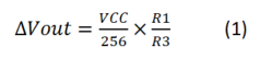
Equation 2 then calculates the output range of Vout:
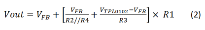
VTPL0102’s range is from 0V to VCC. VFB is the selected shunt regulator’s reference voltage. In the case of the LMV431, the VFB is 1.24V. VCC is the operational amplifier’s power supply and Vout is the adapter output voltage.
USB PD PPS is becoming more and more popular. Configuring the traditional adapter to the PPS function with minimum components and low cost is a challenge, but with some additional circuitry, mobile adapters can easily achieve the PPS function in the latest USB PD technology.