SSZT533 february 2019 LM34936 , LM5176
Printed circuit board (PCB) layout design plays a critical role in achieving high performance for a four-switch buck-boost regulator. In earlier installments of this series, we discussed strategies for placing the regulator’s power components, AC current loop design and current-sense trace routing. In this installment, I will focus on optimal routing of the gate-drive and return paths.
The gate-drive signal for each of the four metal-oxide semiconductor field-effect transistors (MOSFETs) runs along a closed loop. Figure 1 shows the LM34936 or LM5176 four-switch buck-boost controller as an example.
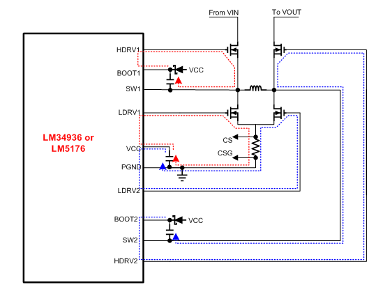 Figure 1 Gate-drive and Return Path
Routes
Figure 1 Gate-drive and Return Path
RoutesIn a real circuit, PCB traces usually have parasitic resistance, inductance and capacitance. The PCB trace capacitance for the gate drive is normally negligible, so I will ignore it here. Figure 2 shows the equivalent gate-drive circuit. RTrace1 is the PCB drive trace resistance, RTrace2 is the drive return trace resistance, LTrace1 is the drive trace stray inductance, LTrace2 is the return path inductance and Ciss is the MOSFET gate input capacitance. The trace resistance and inductances can cause gate signal delays; therefore, it’s best to keep the drive and return traces as short as possible.
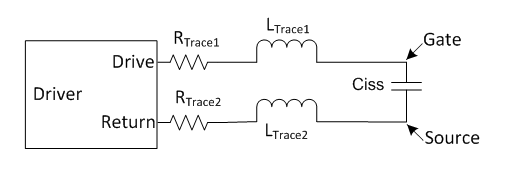 Figure 2 Gate-drive Equivalent
Circuit
Figure 2 Gate-drive Equivalent
CircuitGiven board area limitations, it is not possible to place the driver very close to the MOSFET. Even if the MOSFET is not very close, it is possible to make RTrace1 and RTrace2 <1 Ω in most designs. LTrace1 and LTrace2 can become significant if the trace routing is poor, however. An inductance of just a few nanohenries may resonate wildly with the MOSFET gate capacitance and create gate voltage ringing, as shown in Figure 3. If the magnitude of the ringing exceeds the MOSFET gate threshold voltage, Vth, it will cause unwanted extra switching action and result in severe switching losses inside the MOSFETs.
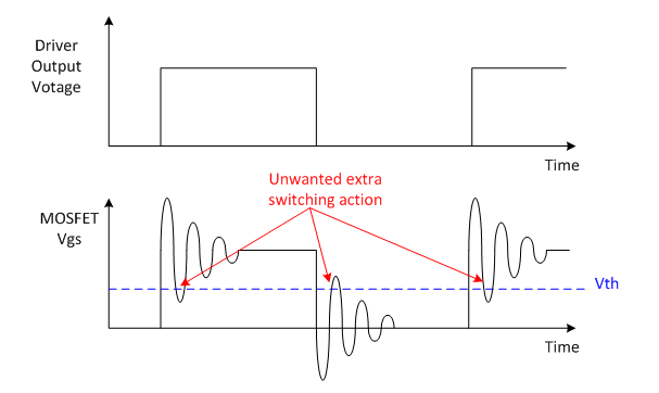 Figure 3 Gate Ringing and Unwanted
Extra Switching Action
Figure 3 Gate Ringing and Unwanted
Extra Switching ActionSo how can you minimize the gate-drive inductance? According to physics, the gate-drive inductance is proportional to the spatial area enclosed by the drive current loop, which is the area defined by the actual drive and return traces. Minimizing the spatial area of the drive current loop should be your main focus in routing the MOSFET drive and return paths.
Assume that the drive is at point A and the MOSFET is at point B on the PCB; the drive trace must be routed from point A to point B and return back to point A. Also assume that a straight trace from A to B is not possible because other components are in the way. Figure 4 shows two different routing patterns. Obviously, option No. 2 encloses a minimal spatial area and thus produces the least inductance, even though the total trace length is the same as option No. 1. This example clearly shows that the optimal routing is to place the drive and return traces closely side by side for the entire distance between the driver and the MOSFET.
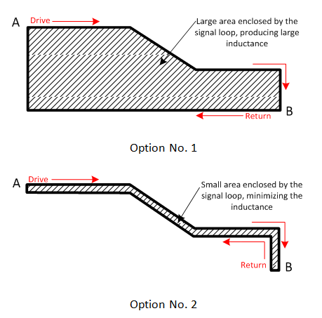 Figure 4 Routing Patterns for Current
Loop Traces between Points a and B on the PCB
Figure 4 Routing Patterns for Current
Loop Traces between Points a and B on the PCBAgain, given board area limitations, sometimes there is no space to place the pair of drive and return traces side by side on the same layer. A solution is to route the return trace in the shadow of the drive trace on an adjacent layer, as shown in Figure 5, where the drive trace runs from point A (Drive) on Layer 1 to point B (MOSFET), and takes the via hole to Layer 2, and runs back to point A in the shadow of the drive trace. In this way, the drive and return traces basically run closely side by side in the vertical direction, minimizing the spatial area enclosed by the signal loop.
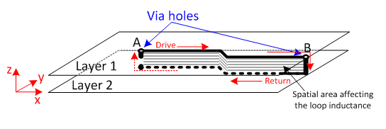 Figure 5 Routing the Return Trace in
the Shadow of the Drive Trace on an Adjacent Layer to Minimize Loop
Inductance
Figure 5 Routing the Return Trace in
the Shadow of the Drive Trace on an Adjacent Layer to Minimize Loop
InductanceYou should apply these schemes, either running side by side or overshadowing, when routing the two high-side MOSFET drive traces, namely the HDRV1/SW1 and HDRV2/SW2 traces. For the two low-side MOSFETs, the two drive return paths run back to the PGND pin. If the PCB has multiple layers that include a ground plane layer, then you just need to route the LDRV1 and LDRV2 traces and let the return path take the ground plane. Because current naturally takes the path with the least impedance, the return path will be virtually in the shadow of the LDRV1 or LDRV2 traces, as depicted in Figure 5.
If the ground layer is not available, then you can route both the drive and return traces side by side on the same layer. There should be two dedicated pairs of traces: one pair of LDRV1/PGND traces and one pair of LDRV2/PGND traces for the two low-side MOSFETs.
Conclusion
In order to optimize four-switch buck-boost performance, keep the gate-drive traces as short as possible. If the PCB space does not allow you to place the MOSFET very close to the drivers, then route the gate-drive signal such that the pair of drive and return traces are placed closely side by side – either on the same PCB layer or on adjacent layers – to minimize the spatial area enclosed by the drive signal loop. Doing this minimizes the parasitic inductance, prevents gate-drive ringing, minimizes switching losses and achieves high performance for a four-switch buck-boost converter.