SSZT499 april 2019 OPA1671
A high-fidelity audio signal chain gains several advantages when the system supply voltages are higher – the signal-to-noise ratio, dynamic range and slew rates can all improve with increasing supply voltages. But constraints from battery- and USB-powered systems or limitations on the audio analog-to-digital converter or codec may require signal processing with low-voltage supplies.
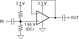
Picking an amplifier for these applications isn’t always straightforward. An amplifier built with bipolar technology gives the best possible combination of noise and quiescent current, but has a limited input and output signal dynamic range. Consider a basic amplifier configured as a buffer on a 3.3-V rail. Without a rail-to-rail input, the input signal range is typically limited by 1.2 V. The output stage can also limit the dynamic range. Figure 1 below shows a typical AC-coupled op-amp configuration, with the common mode voltage biased at mid-rail.
 Figure 1 Input and Output Voltage
Swing
Figure 1 Input and Output Voltage
SwingNominal consumer audio line-level input voltages are -10 dBV; designing for an additional 10-dB headroom gives a peak-to-peak input voltage of 2.828 V. In order to buffer or filter a signal of this magnitude with only a 3.3-V supply rail, an audio-grade, rail-to-rail input CMOS amplifier is required. Additionally, professional wireless microphones must deliver high-fidelity audio within small-sized solutions capable of more than 8 hours of battery operation. These systems require small-form-factor solutions with low quiescent current and extremely low noise floors to enable extended portable operation and high-fidelity audio recording.
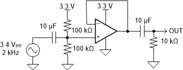
In addition to merely limiting the voltage, a bipolar output can have a significant increase in quiescent current when the output is in saturation and can show significant delay when recovering from output overload, leading to harsh harmonics when the signal is at or near the point of clipping. In Figure 2, a schematic example of an overdriven amplifier is given.
 Figure 2 AC-coupled, Unity Gain Audio
Amplifier Schematic Example
Figure 2 AC-coupled, Unity Gain Audio
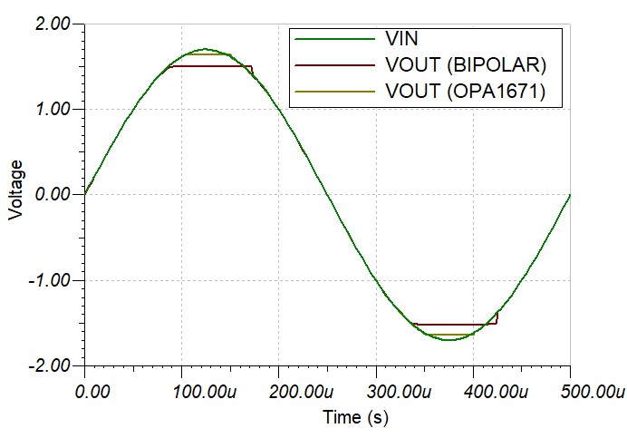
Amplifier Schematic ExampleFigure 3 shows the output of the amplifier in Figure 2, simulated using circuit models. For the simulation, the amplifier input signal is driven beyond the rails for two different amplifiers: a standard, 3-MHz, rail-to-rail input/bipolar output amplifier and a new 13-MHz, rail-to-rail input/output CMOS amplifier from TI, the OPA1671.
 Figure 3 Transient Simulation of
Clipping on a Bipolar vs. CMOS Amplifier
Figure 3 Transient Simulation of
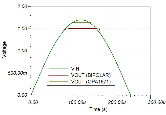
Clipping on a Bipolar vs. CMOS AmplifierIn Figure 4, the simulation zooms in closely to the peaks where it is easy to see that not only does the CMOS amplifier exhibit a wider output voltage swing before clipping, but the wide bandwidth and CMOS outputs allow for a much faster recovery from clipping.
 Figure 4 Transient Simulation of
Clipping on a Bipolar Amplifier vs. a CMOS Amplifier
Figure 4 Transient Simulation of
Clipping on a Bipolar Amplifier vs. a CMOS AmplifierMany CMOS amplifiers improve on the headroom limitations of bipolar amplifiers thanks to lower threshold and saturation voltages inherent in CMOS processes. However, voltage noise, total harmonic distortion (THD) and output impedance will typically be compromised.
The OPA1671, a rail-to-rail input and output CMOS audio amplifier, helps provide a solution to these design challenges by providing ultra-low noise, THD and wide bandwidth (13 MHz). The rail-to-rail input and outputs, along with the high input impedance, enable wide signal swings in buffer configurations. The low current and voltage noise, coupled with a low 1.25-mV offset voltage, make the OPA1671 an excellent amplifier for high-gain preamplifier circuits that maximize output swing and can provide very low output-impedance drive to an audio ADC or codec.