SSZT491 April 2019 LMR33630 , TPS7A33
The first installment of this two-part series demonstrated how to create a tracking pre-regulator for a positive output low-dropout regulator (LDO). In this installment, we’ll use a similar technique to create a tracking pre-regulator for a negative output LDO. This example will use the same LMR33630 evaluation module (EVM), but in the inverting buck-boost configuration in conjunction with the TPS7A3301 LDO.
One sample application for a negative LDO is to provide a negative voltage rail for an amplifier. Figure 1 shows a modification to the LMR33630 feedback network in order to create pre-tracking regulator for negative output LDO.
 Figure 1 A Negative-tracking
Pre-regulator with the LMR33630 and TPS7A3301
Figure 1 A Negative-tracking
Pre-regulator with the LMR33630 and TPS7A3301Modifying the TPS7A3301 EVM feedback resistor generates a -5-V output at the LDO; the LDO output voltage connects to the base of the 2N3904 N-channel P-channel N-channel (NPN) transistor. The LMR33630 internal reference voltage is 1 V with respect to the GND pin. Therefore, the voltage at the FB pin of the LMR33630 will be regulated at 1 V with respect to the GND pin of the device, which is now the negative output of the DC/DC converter.
As shown in Figure 1, the voltage across RFBB is also equal to 1 V. This in turn will create a reference current flowing in RFBB with a value of IFBB = 1 V/1 kΩ = 1 mA.
This IFBB reference current will then be mirrored by Q1/Q2-matched P-channel N-channel P-channel (PNP) transistors to generate the collector of Q3, which flows through resistor R1 (IC ≈ IE of Q3).
With IFBB ≈ IR1 ≈ 1 mA and approximating to 0.6 V, you can then calculate the expected output voltage of the DC/DC converter as:
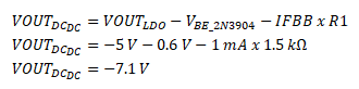
In this case, the voltage output of the DC/DC converter stage will be approximately 2.1 V lower than the output voltage of the LDO.
As you can see from the calculation, it’s possible to approximate the voltage difference between the input and output of the LDO with Equation 1:
During design, you have to make sure that the DC/DC converter provides enough negative voltage to start up an LDO. Choosing a proper value for the R1 resistor can control this voltage.
In this example, the TPS7A3301 has a typical undervoltage lockout of -2 V. When the LDO is still off, and the input of the DC/DC converter is applied, the output of the LMR33630 will start going negative while the output of the LDO is still at 0 V.
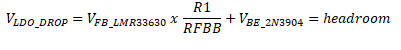
The initial current that flows in the Q2 in Figure 1 is approximately 1 mA (1 V/1 kΩ). During initial startup and also illustrated in Figure 2, the VOUT DC/DC voltage is:
As you can see, you have to choose a proper value of resistor R1 to generate a sufficient voltage to start up the LDO that a user choose in their application.
 Figure 2 Initial Startup Voltages off
the LMR33630 and TPS7A3301
Figure 2 Initial Startup Voltages off
the LMR33630 and TPS7A3301Figure 3 and Figure 4 illustrate the startup and shutdown waveforms for the example negative-tracking pre-regulator circuit.
") Figure 3 Startup Waveform for a 12-v
Input at the DC/DC Converter (CH1 = Vin, CH2 = Voutldo, CH3 = Voutdcdc, CH4 =
Ioutldo)
Figure 3 Startup Waveform for a 12-v
Input at the DC/DC Converter (CH1 = Vin, CH2 = Voutldo, CH3 = Voutdcdc, CH4 =
Ioutldo)") Figure 4 Zoomed-in Startup Waveform for
a 12-v Input at the DC/DC Converter (CH1 = VIN, CH2 = VOUTLDO, CH3 = VOUTDCDC,
CH4 = IOUTLDO)
Figure 4 Zoomed-in Startup Waveform for
a 12-v Input at the DC/DC Converter (CH1 = VIN, CH2 = VOUTLDO, CH3 = VOUTDCDC,
CH4 = IOUTLDO)In Figure 3 and Figure 4, the output of the DC/DC converter is 1.925 V lower than the LDO. There is a small discrepancy between the calculations and experimental value (1.925 V vs. 2.1 V); this is due to the matching current in the PNP pair. Having a co-packaged PNP improves this matching compared to a discrete type, but there will be a small discrepancy in the current between the pair. One way to improve the matching is to make a Wilson current mirror to generate the reference current, as described in Akshay Mehta’s blog post, “How to Create a Programmable Output Inverting Buck-Boost Regulator.”
Figure 5 through 8 are some scope captures on the shutdown performance of the circuit shown on Figure 2. Figure 9 shows the modified LMR33630EVM and TPS7A3301EVM PCB board in order to implement the tracking functionality.
") Figure 5 Shutdown Waveform for a 12-v
Input at the DC/DC Converter (CH1 = VIN, CH2 = VOUTLDO, CH3 = VOUTDCDC, CH4 =
IOUTLDO)
Figure 5 Shutdown Waveform for a 12-v
Input at the DC/DC Converter (CH1 = VIN, CH2 = VOUTLDO, CH3 = VOUTDCDC, CH4 =
IOUTLDO)") Figure 6 Zoomed-in Shutdown Waveform
for a 12-v Input at the DC/DC Converter (CH1 = VIN, CH2 = VOUTLDO, CH3 =
VOUTDCDC, CH4 = IOUTLDO)
Figure 6 Zoomed-in Shutdown Waveform
for a 12-v Input at the DC/DC Converter (CH1 = VIN, CH2 = VOUTLDO, CH3 =
VOUTDCDC, CH4 = IOUTLDO)") Figure 7 Load-transient Waveform at the
Output of the LDO with a 200-mA Step Load (CH1 = VIN, CH2 = VOUTLDO
[AC-coupled], CH3 = VOUTDCDC [AC-coupled], CH4 = IOUTLDO)
Figure 7 Load-transient Waveform at the
Output of the LDO with a 200-mA Step Load (CH1 = VIN, CH2 = VOUTLDO
[AC-coupled], CH3 = VOUTDCDC [AC-coupled], CH4 = IOUTLDO)") Figure 8 Load-transient Waveform at the
Output of the LDO with a 500-mA Step Load (CH1 = VIN, CH2 = VOUTLDO
[AC-coupled], CH3 = VOUTDCDC [AC-coupled], CH4 = IOUTLDO)
Figure 8 Load-transient Waveform at the
Output of the LDO with a 500-mA Step Load (CH1 = VIN, CH2 = VOUTLDO
[AC-coupled], CH3 = VOUTDCDC [AC-coupled], CH4 = IOUTLDO) Figure 9 Board Picture for a
Negative-tracking Pre-regulator
Figure 9 Board Picture for a
Negative-tracking Pre-regulatorTogether with a positive-tracking pre-regulator, you can see that both circuits can increase your system efficiency when you are designing something that requires an LDO as your point-of-load power supply.