SSZT485 May 2019 TPS568230
Driven by the global cloud computing development and continuing construction of data centers, shipments of global storage equipment are experiencing explosive growth. As the key part of the storage equipment, the demands for DC/DC converters that power the storage equipment (solid-state drive [SSD] and memory) also show a relatively rapid growth trend.
Figure 1 shows a simplified power architecture for an enterprise solid-state drive (SSD). The first stage is the protection and backup circuit; the input voltage of this application is normally 12 V. The second stage requires DC/DC converters for higher current (>6 A). In the third stage, low-dropout regulators are added in the rails, which are very sensitive to voltage fluctuations.
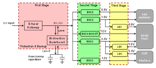 Figure 1 A Simplified Power
Architecture of an Enterprise SSD
Figure 1 A Simplified Power
Architecture of an Enterprise SSDIn this SSD, the DC/DC converters need to fulfill several requirements: small output voltage fluctuation, high efficiency and small solution size.
Except for those very sensitive rails, the rest of the power rails supplied by buck converters also need less voltage output fluctuation To not only support the low output voltage ripple in constant load (less than 1% * VOUT even at full load), but also provide a small overshoot/undershoot in load transient. This is because large voltage fluctuations will have a risk of NAND deterioration and controller instability, which will shorten system lifetimes or even cause damage.
There is no exception that efficiency is an important indicator for DC/DC converters in most applications. High efficiency can prevent power loss and improve thermal performance. High efficiency is also very critical for SSDs because excessive temperatures will slow down input/output per second and could damage the SSD.
With the explosive growth of data, engineers want to put more and more storage units in one data center. This also challenges the solution size of DC/DC converters. Not only does it require a smaller size to provide higher power density, but it also has more demanding requirements for height.
Given these demanding requirements – especially the output ripple – engineers will add more and more capacitors (200 -~500 µF in 8 A) in the output to keep the ripple at a small voltage. But adding more capacitors will not only attenuate the performance of the load transient, it will expand the solution size and increase the bill-of-materials cost. So there has to be a trade-off between the output stability and solution size, even though a larger solution size can help thermal dissipation.
Figure 2 is a schematic of TI’s newly released TPS568230. It is an 18-VIN, 8-A buck converter with D-CAP3™ control mode that provides a fast transient response with no external compensation components and an accurate output voltage. It can achieve an output ripple that is less than 10 mV at full load and also a faster load transient response with only four pieces of 22 µF *4pcs at a 600-kHz switching frequency, as shown in Figure 3. The load step is from 2 A to 6 A with a 2.5 A/µS slew rate. The peak-to-peak output voltage ripple is only 55 mV, which can effectively avoid the NAND deterioration and associated damage risks.
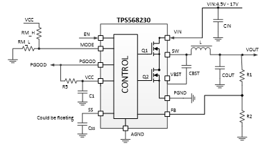 Figure 2 TPS568230 Step-down Converter
Schematic
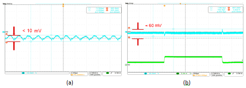 Figure 3 Output Ripple with Full Load
(a); Load Transient Performance (b) (vIN = 12 V, vOUT =
1.05 V, FSW = 600 Khz)
Figure 3 Output Ripple with Full Load
(a); Load Transient Performance (b) (vIN = 12 V, vOUT =
1.05 V, FSW = 600 Khz)With low RDS(on) (19.5 mΩ high side, 9.5 mΩ low side), the TPS568230 offers good efficiency. Figure 4 shows the thermal performance.
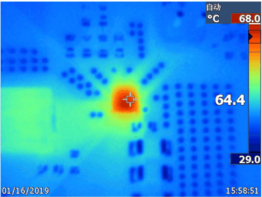 Figure 4 TPS568230 Thermal Performance
(vIN = 12 V, vOUT = 1.05 V, IOUT = 8 A,
FSW = 600 kHz, 10 Minutes)
Figure 4 TPS568230 Thermal Performance
(vIN = 12 V, vOUT = 1.05 V, IOUT = 8 A,
FSW = 600 kHz, 10 Minutes)The package size of the TPS568230 is only 3 mm by 3 mm2 and the highest 1-MHz switching frequencies can also help adapt to high power-density applications. Particularly worth mentioning is that at a 1.05-V output voltage and 1-MHz switching frequency, the value of the inductor is only 0.33 µH (Würth: 744373240033, 4.45 mm by 4.06 mm by 1.8 mm), which can save both power solution size and height. Figure 5 is a model of the printed circuit board. The total solution size is less than 185 mm2 and the height is less than 2 mm.
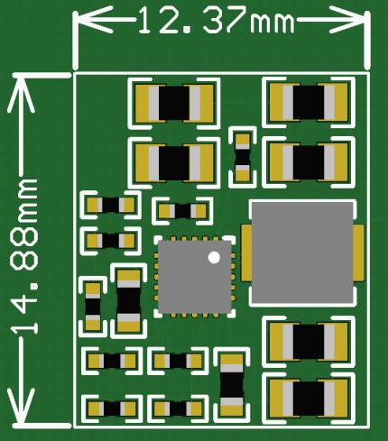 Figure 5 Solution Size with 1-MHz
Switching Frequency
Figure 5 Solution Size with 1-MHz
Switching FrequencyThe TPS568230 satisfies fast load transient and high power-density requirements, as well as decreasing bill-of-materials cost. It’s a good fit for storage applications as well as routers, switches and servers that have similar power rail requirements.
Additional Resources:
- View the TPS568230 datasheet
- Take our online training: DC/DC Buck Converters: What do all of these features mean?