SSZT444 july 2019
You are on a quest to design an active filter. You have the specifications of the filter’s frequency response, but how do you create a circuit that does just what you want?
If you took the conventional approach, you would need to manipulate the second-order control system equations by consulting multiple filter-response coefficient tables; plot and compare multiple filter responses; select the filter response that best meets your specification; choose a circuit topology and calculate the passive component values by solving complex quadratic equations; and pick standard, graded passive components and an operational amplifier (op amp) that closely match the calculated values. You’ll need to repeat component selection and calculations until you achieve the desired performance – a process that could easily take weeks, if not months.
TI’s Filter Design Tool streamlines the system design, circuit design and circuit verification process and helps you select a filter circuit that has high chance for first-pass success.
| Designing a robust filter circuit, made easy | |
|
Design, optimize and simulate complete multistage active filter solutions within minutes. Launch the tool now. |
The Filter Type tab in the tool (Figure 1) gives you the option to select low-pass, high-pass, band-pass, band-stop (notch) or all-pass filters.
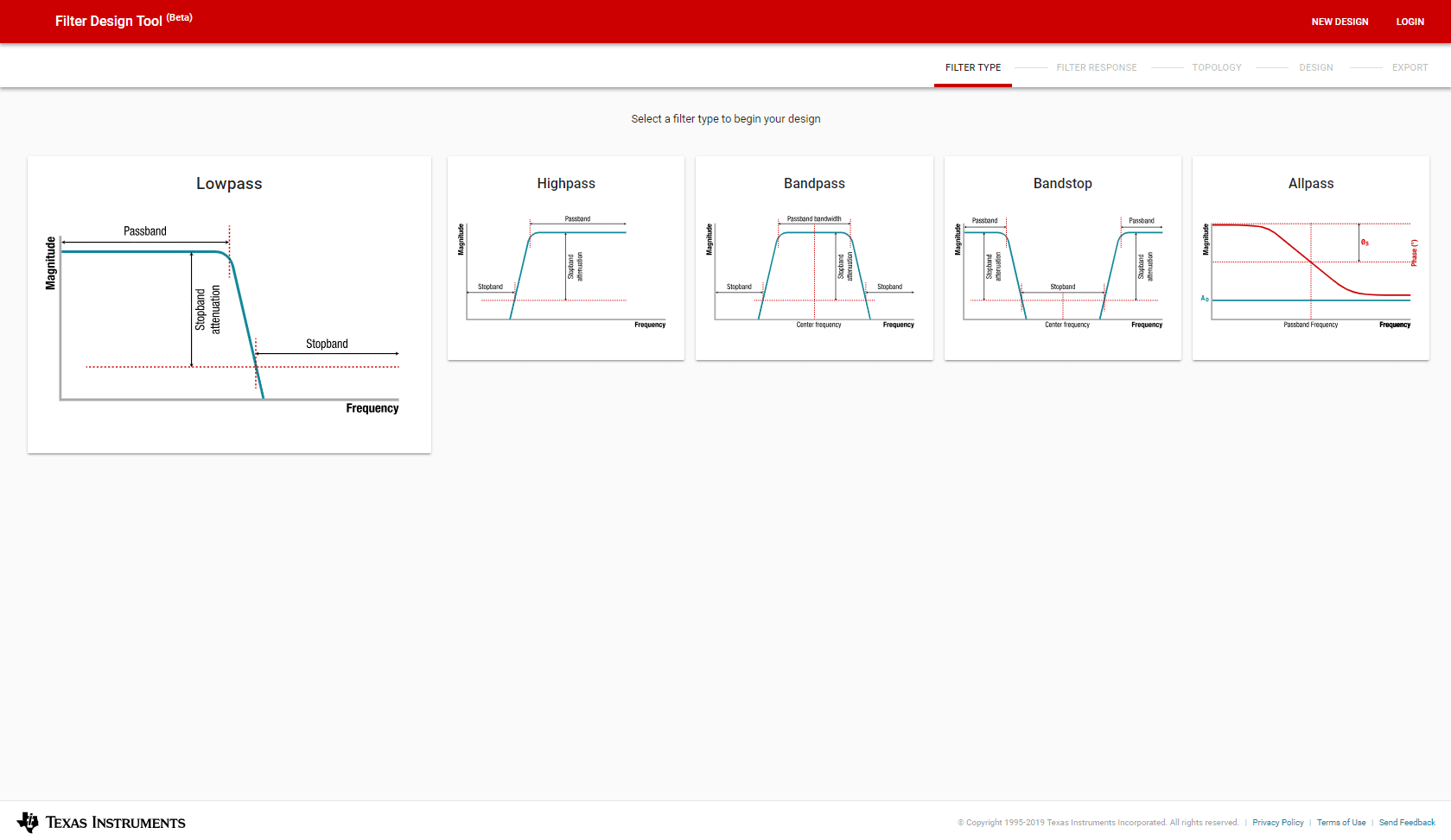 Figure 1 Filter Type Selection
Screen
Figure 1 Filter Type Selection
ScreenClick one of the filter types to move forward to the Filter Response screen (Figure 2).
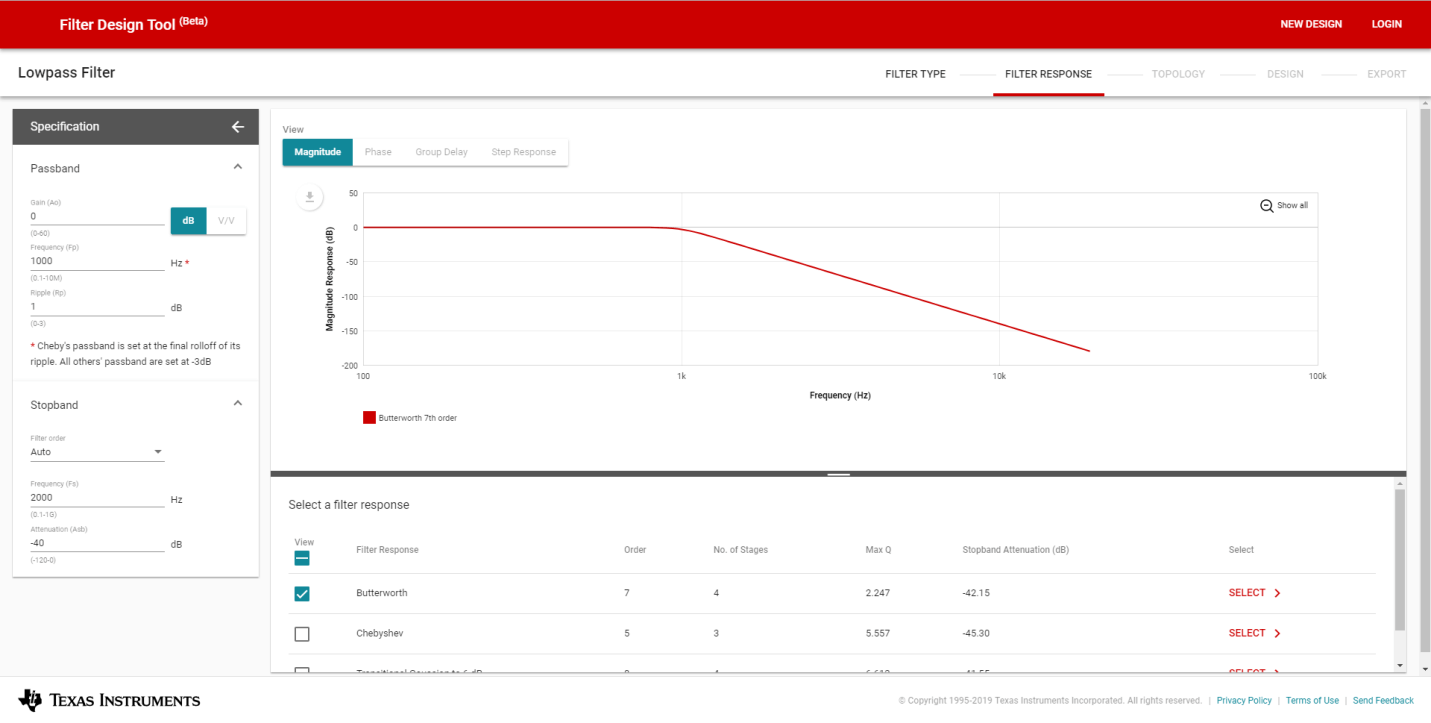 Figure 2 Filter Response Screen
As you enter your design specifications on the left, the chart on the right updates the waveform to reflect the characteristics of your selected filter response. You can switch between magnitude, phase, group delay and step response by clicking the button above the chart.
The table beneath the waveform presents the filter responses that meet your design specifications. The first filter response is displayed by default, but you can check or uncheck multiple other filter responses to compare or hide their characteristics and performance.
To advance to the Topology screen (Figure 3), click Select to the right of the filter response you want.
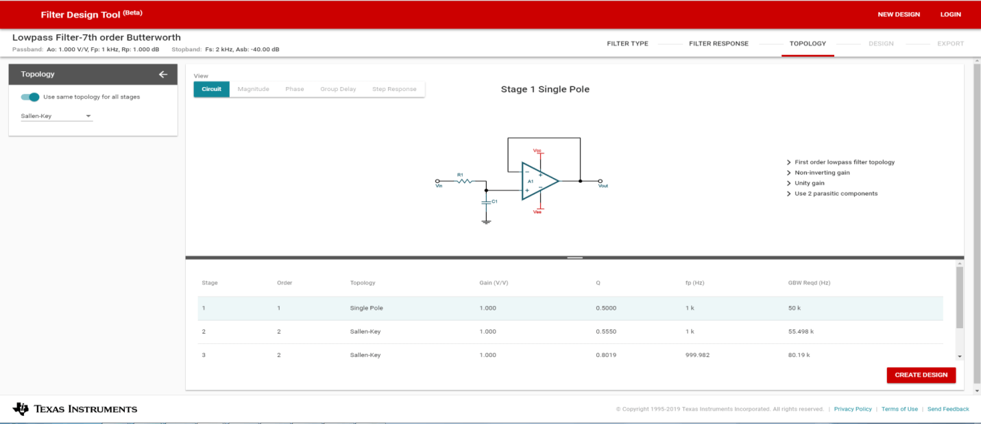 Figure 3 Topology Screen
The Filter Design Tool currently supports Sallen-Key and Multiple Feedback topologies for low-, high- and band-pass filters. Band-stop filters only supports Bainter topology because of the challenges in suppressing ringing within the stop-band region for Sallen-Key topology, and the difficulty in meeting the gain and natural frequency for the Multiple Feedback topology.
The Filter Design Tool recommends the best topology based on your filter specification and applies this circuit to all stages. You have the option to choose an alternate topology to meet your design priorities. Toggling the “Use same topology for all stages” switch gives you the ability to mix and match topologies, as shown in Figure 4.
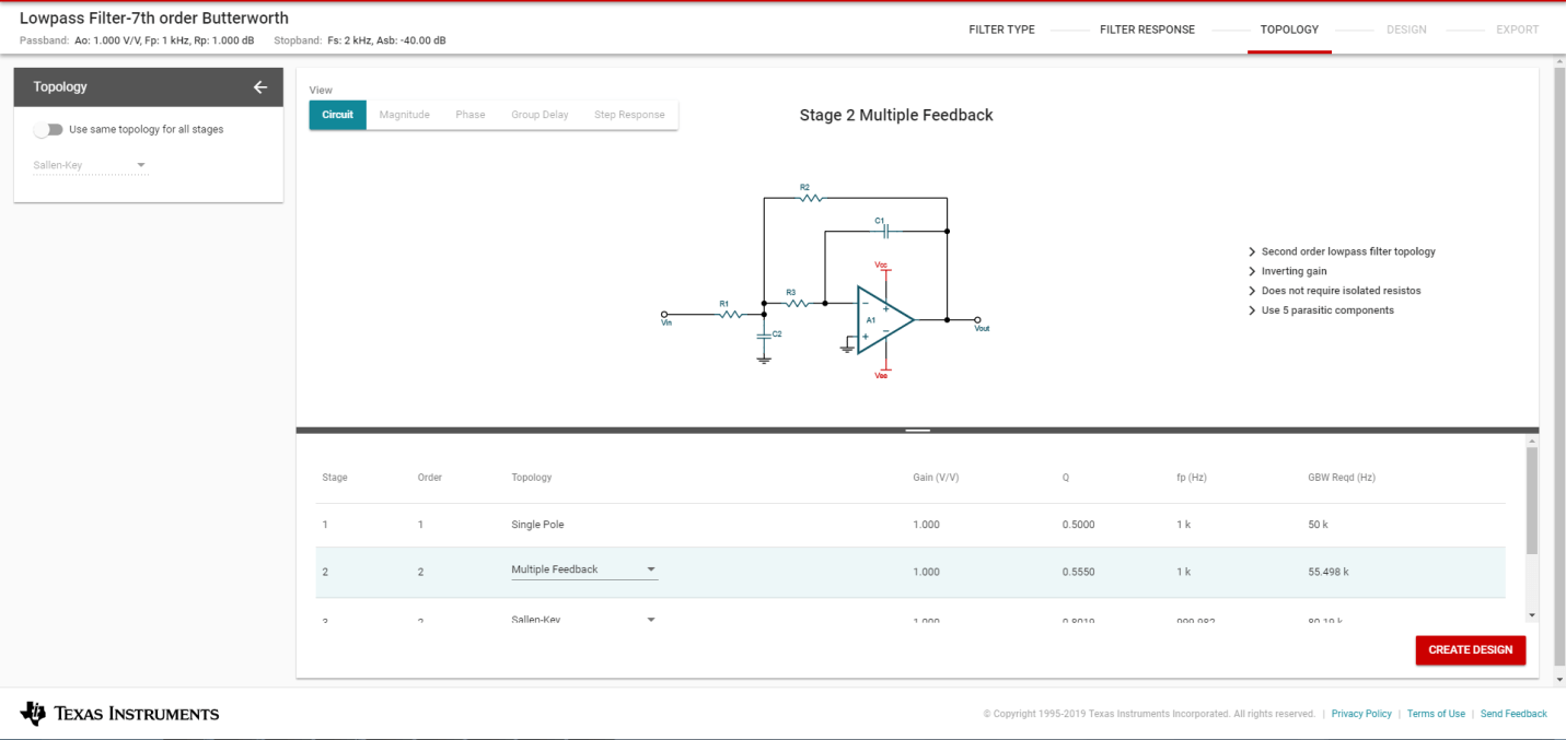 Figure 4 Customize Circuit Topology for
Each Stage
Figure 4 Customize Circuit Topology for
Each StageYou can observe the characteristics of each stage by clicking a particular row in the table, as shown in Figure 5. Advanced users could potentially rearrange the circuit sequence in the exported TINA-TI™ software schematic to meet their design priorities.
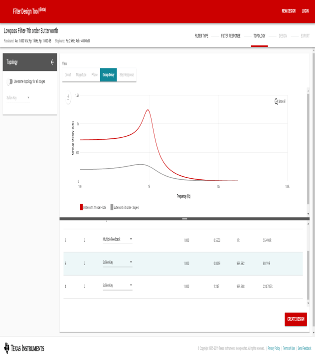
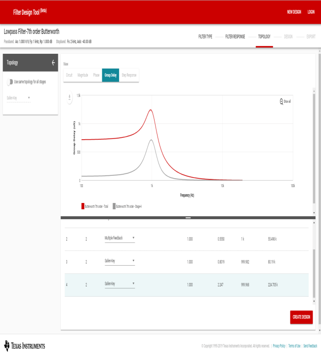 Figure 5 Evaluate Characteristics of
Each Stage
Figure 5 Evaluate Characteristics of
Each StageThe Design tab (Figure 6) lets you quickly complete three crucial design steps: schematic creation, op amp selection and component tolerance analysis.
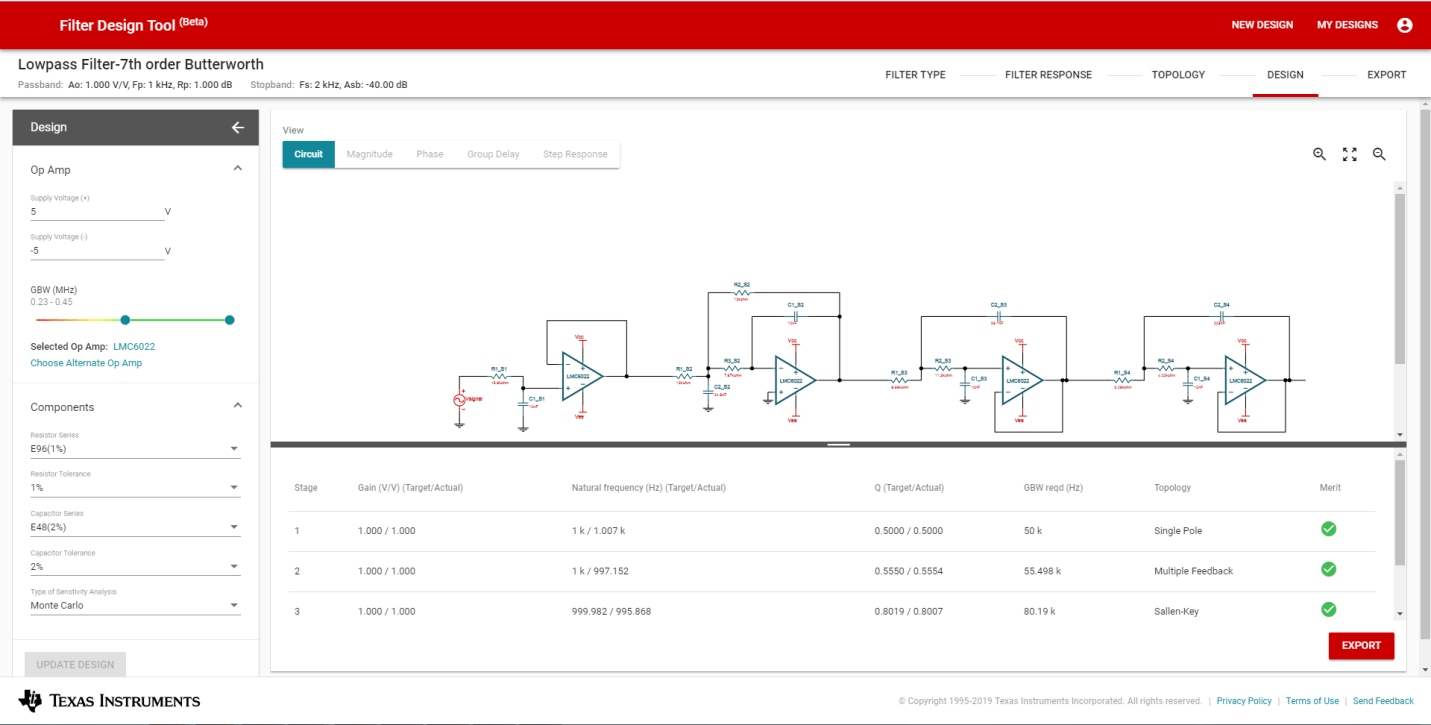 Figure 6 Design Screen
The complete schematic with the actual amplifier and passive components is displayed on the Design screen. The tool uses the standard resistor and capacitor values that closely match the calculated values. It is always a design challenge to balance between performance and component cost.
The default power supply is ±5 V and can be easily updated on the top left window of the design screen. The gain bandwidth slider range is set to 10 to 200 times the calculated gain bandwidth. The left slider bar is set to the recommended 100 times the calculated gain bandwidth by default. You can lower the gain bandwidth margin by sliding it to the left, to the yellow and red region of the heat map.
It’s good practice to perform a simulation if you choose a lower gain-bandwidth amplifier. If you have a specific design priority such as low power, high precision or number of lanes, you can click Select Alternate Op Amp on the design screen. This brings you to a dedicated op-amp selection screen, as shown in Figure 7. On this screen, you will be able to specify your design priorities and pick the best TI op amp for your design. Click Select to pick your op amp or Cancel to return to the Design screen.
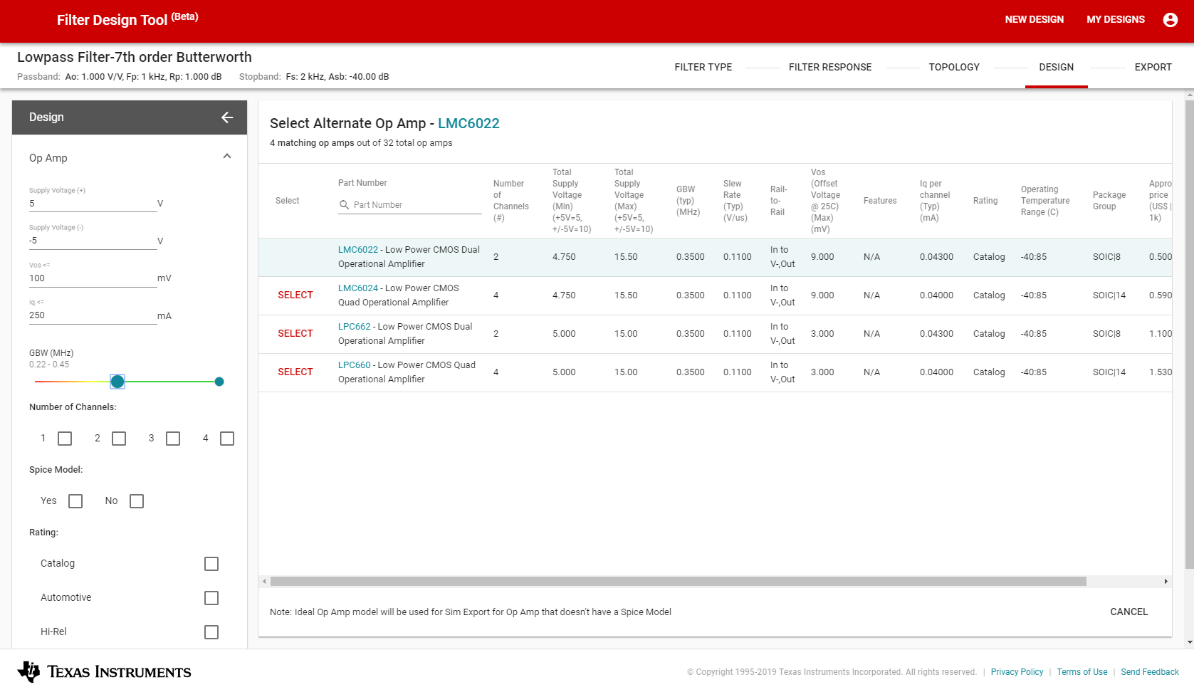 Figure 7 Select Alternate
Amplifier
Figure 7 Select Alternate
AmplifierThe default resistor and capacitor grades are set to ensure that the deviation between the actual and target values is less than 5% for gain, natural frequency and Q. You can trade off performance and accuracy by choosing a lower-grade capacitor and resistor for reduced costs. The tool will recalculate the actual gain, natural frequency and Q with your new selection. If any of the values deviate more than 5%, the circle of the last column on the table will turn from green to yellow. If the deviation is greater than 10%, the circuit will turn red on the design screen as shown in Figure 8.
The rule of thumb to achieving high accuracy and low cost is to lower the grade for the passive components and still keep the color of the circles green. If you must operate within yellow or red, export the design and run a thorough analysis to ensure that the design still meets your specifications.
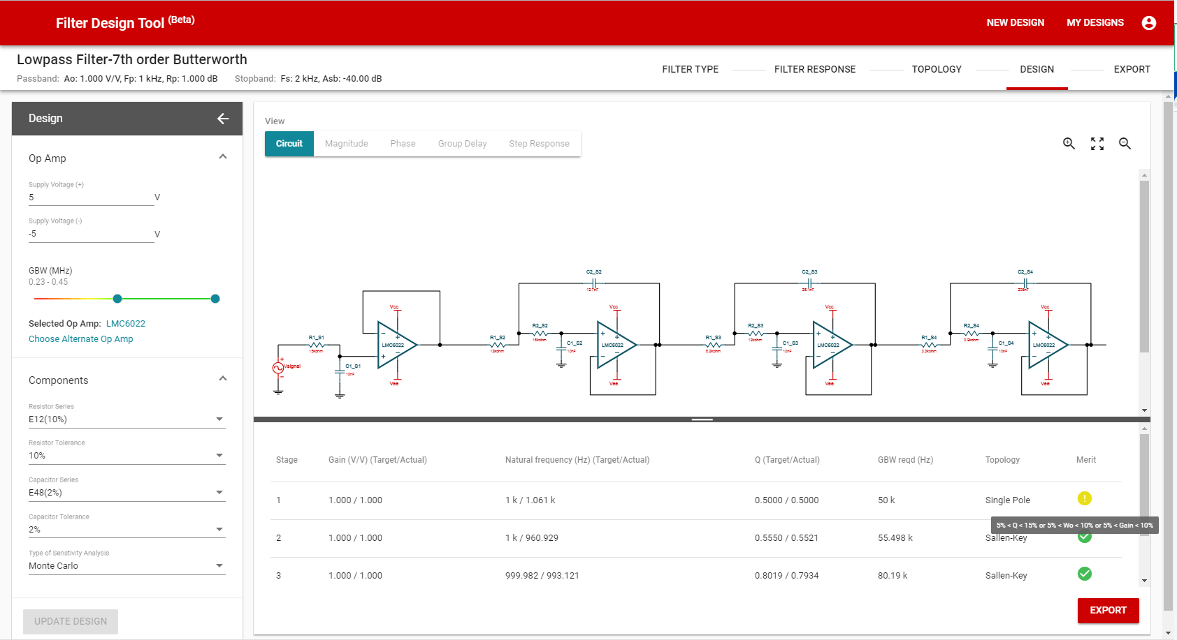 Figure 8 Use Merit as a Quick
Performance Indicator
Figure 8 Use Merit as a Quick
Performance IndicatorOnce you have successfully created and analyzed your design, you can export the design information to a PDF report, and the schematic to TINA-TI software as shown in Figure 9. It’s also a good idea to perform a Spice simulation, as not all the op-amp characteristics have been included in the design considerations.
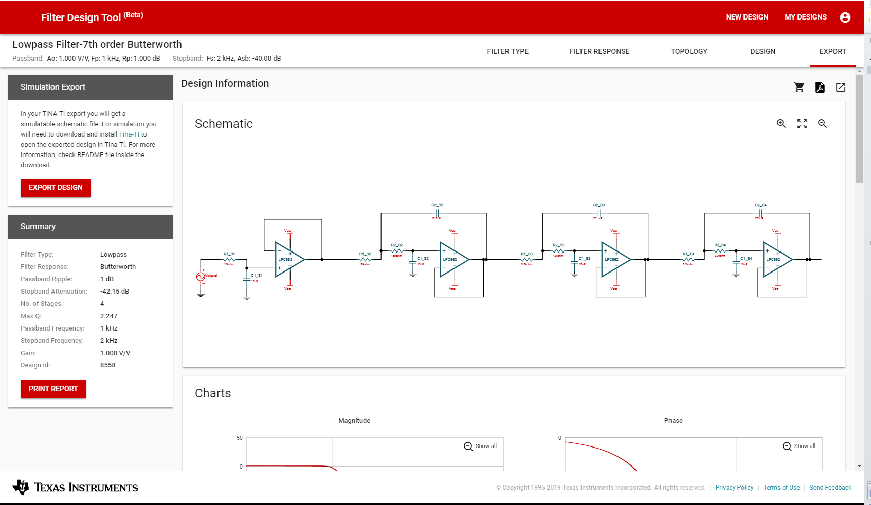 Figure 9 Export Screen
The new Filter Design Tool has a simple user interface powered by intelligent and computation-intensive algorithms. It drastically enhances your experience in designing a robust filter circuit from the first step to the last.