SSZT348 January 2020
Many textbooks and reference guides define operational amplifiers (op amps) as special integrated circuits (ICs) that perform various functions or operations, such as amplification, addition and subtraction. While I agree with this definition, it’s also important to note the importance of the voltages at the input pins of the device.
When the input voltages are equal, the op amp is usually operating linearly, and it is during linear operation that the op amp accurately performs the aforementioned functions. However, an op amp can change only one thing to make the input voltages equal: the output voltage. Therefore, the output of an op amp circuit is typically connected in some manner to the input, which is commonly referred to as voltage feedback.
In this article, I will explain the basic operation of a general-purpose, voltage-feedback op amp and refer you to other content where you can learn more.
| Designing with op amps | |

|
Explore TI Precision Labs, our on-demand training for analog engineers. |
Figure 1 depicts the standard schematic symbol for an op amp. There are two input terminals (IN+, IN-), one output terminal (OUT) and two power-supply terminals (V+, V-). The names for the terminals may vary from manufacturer to manufacturer or even within a single manufacturer, but they’re the same five terminals nonetheless.
For example, you may see Vcc or Vdd instead of V+. Similarly, you may see Vee or Vss instead of V-. Other labels for the power-supply terminals will differ because they refer to the types of transistors inside the device. For example, when using bipolar junction transistors (BJTs) inside of op amps, the power supplies correspond to the collector and emitter terminals of the BJTs: Vcc and Vee. When using field-effect transistors (FETs) inside op amps, the power-supply labels correspond to the drain and source of the FETs: Vdd and Vss. Today, many op amps contain both BJTs and FETs, so V+ and V- are common labels, regardless of the transistors inside the device. In short, don’t get caught up on the pin labels; just understand what they do.
 Figure 1 General-purpose Op-amp
Schematic Symbol
Figure 1 General-purpose Op-amp
Schematic SymbolEquation 1 expresses the transfer function of an op amp:
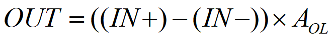
In Equation 1, AOL is known as the “open-loop gain,” and it is generally an extremely large value in modern op amps (120 dB, or 1,000,000 V/V). As an example, if the voltage difference between IN+ and IN- is just 1 mV, the op amp will try to output 1,000 V! In this configuration, the op amp is not operating in a linear region because the output is not able to make the inputs equal to one another (remember, ideally IN+ equals IN-). Therefore, op amps need a way to control the open-loop gain, which is done with negative feedback.
Figure 2 depicts an op amp as part of a feedback control system. You will notice that the output, OUT, is fed back to the negative input, IN-, through a block labeled ß. ß is known as the feedback factor, and generally uses resistors to divide down the output voltage.
 Figure 2 Op Amp with Negative
Feedback
Figure 2 Op Amp with Negative
FeedbackFigure 3 compares an op amp operating in open loop versus one with negative feedback. These TINA-TI™ software simulations use a nearly ideal op amp with power supplies in order to limit the output voltage. Notice that for the open-loop configuration on the left, the output is nearly equal to the positive power supply (V+). This is because there is a small difference (100 mV) between the input pins. This small voltage is amplified by the open loop gain, which forces the output to one of the supply voltages. In the negative feedback or closed-loop version on the right side of Figure 3, the voltage divider on the output of the op amp necessitates an output voltage of 200 mV in order to make the inverting and noninverting inputs equal.
 versus
Negative Feedback (Right)") Figure 3 Open Loop (Left) versus
Negative Feedback (Right)
Figure 3 Open Loop (Left) versus
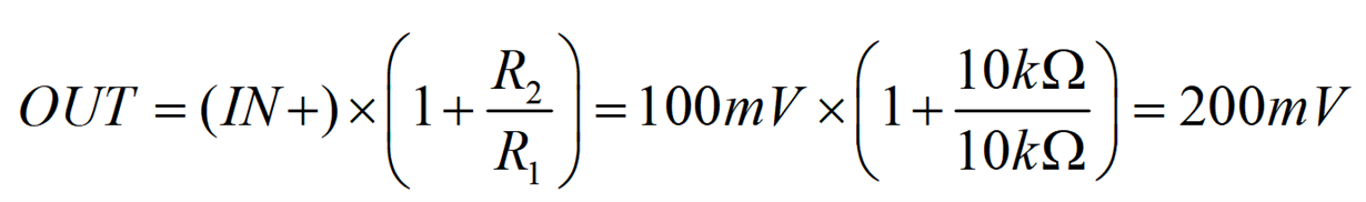
Negative Feedback (Right)The amplification of the input voltage is known as gain. It is a function of the resistor values in the feedback loop. Equation 2 depicts the gain equation for the circuit on the right in Figure 3, which is known as a noninverting amplifier. You’ll see that the calculated output voltage corresponds to the simulation. If you’re interested in learning more about this circuit (and other common op-amp circuits like the buffer, inverting amplifier and difference amplifier), you can download the e-book, the “Analog Engineer’s Circuit Cookbook: Amplifiers.”
The output of an op amp is limited by the supply voltages. Figure 4 is a plot of the output voltage versus the input voltage of the noninverting amplifier in Figure 3. Notice the limitation where the output saturates as it approaches the positive and negative supplies.
 Figure 4 Output versus Input Voltage
for a Noninverting Amplifier Circuit
Figure 4 Output versus Input Voltage
for a Noninverting Amplifier CircuitDue to this limitation, you’ll see in Figure 5 that the voltage difference between the input pins, Vdiff, increases as the output approaches the supplies. It is only when the inputs are nearly equal that the op amp is operating in a linear region.
 Figure 5 Vdiff Versus in+
for a Noninverting Amplifier Circuit
Figure 5 Vdiff Versus in+
for a Noninverting Amplifier CircuitIn order to understand op amps at a deeper level, check out our analog curriculum, TI Precision Labs. This curriculum delves further inside the op amp and discusses fundamental nonidealities such as input offset voltage (Vos), input bias current (IB) and input/output limitations. There are also lectures on advanced topics such as op amp bandwidth (BW), slew rate (SR), noise, common-mode rejection ratio (CMRR), power supply rejection ratio (PSRR) and stability. In addition to lectures, some of the topics have hands-on lab experiments. In order to conduct these experiments, you’ll need the corresponding op-amp evaluation module.
If you’re more of a tinkerer at heart, you may be interested in the Universal Do-It-Yourself (DIY) Amplifier Circuit Evaluation Module (for single-channel devices), the Dual Channel Universal Do-It-Yourself (DIY) Amplifier Circuit Evaluation (for dual-channel devices) or the DIP Adapter Evaluation Module (which can be used in conjunction with a standard prototyping board or breadboard). The DIY EVMs support a variety of packages and have a number of standard op-amp circuits, such as the noninverting amplifier described in this article, inverting amplifier, buffer and filters (both Sallen-Key and multiple feedback). Because the dual in-line package (DIP) adapter EVM converts many standard surface-mount packages to DIP for use in conjunction with a breadboard, you can evaluate just about any amplifier in just about any configuration.
So that’s the fundamental principle of an op amp: it is only linear when the voltages at the input pins are equal. In order to achieve this, however, an op amp can only adjust its output voltage. Output swing limitations can cause the input voltages to diverge from one another, which yields nonlinear, undesirable behavior.
Additional resources
- Download the analog engineer’s calculator and “Analog Engineer’s Pocket Reference.”
- Explore TI's broad portfolio of op amps.