SSZT269 july 2020 BQ25616 , BQ25619 , BQ2970 , BQ2971 , BQ2972 , BQ2973 , LP5012 , TL431 , TLV733P , TPA6203A1 , TPS61169 , TPS7A03 , UCC28910 , UCC28911
An ultraviolet (UV) sterilization box is designed to use UV rays to kill bacteria. UV LEDs can produce UV rays of 260 nm to 280 nm, which can break the bacteria DNA/RNA strand and kill bacteria completely, with a sterilization rate as high as 99%.
LED ultraviolet sterilization technology, first used by astronauts to disinfect water on space missions, is now applicable in our daily lives. Strong LED UV energy can also decompose the molecular structure of odors and effectively remove the musty odor of everyday objects such as glasses, watches and more, sterilizing them as well.
Figure 1 shows a system design of a UV sterilization box with a battery. The battery version is popular with consumers who travel often because the box is portable.
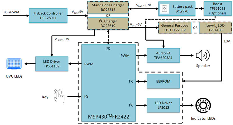 Figure 1 System block diagram of a UV
sterilization box with a battery
Figure 1 System block diagram of a UV
sterilization box with a batteryThis article will highlight TI devices in a UV sterilization box, and explain how the strength of these devices can help resolve some of the challenges in this particular application.
Power-supply scheme
The UCC28911 product family has a flyback controller with FM and AM hybrid control, which integrates 700-V metal-oxide semiconductor field-effect transistors (MOSFETs) and supports a 85- to 265-VAC bus voltage range. The UCC28910 can achieve a maximum output power of 9.5 W, while the UCC28911 can achieve a maximum output power of 12 W.
- Low frequency operation, which improves efficiency at light loads.
- Valley switching, which reduces switching losses.
- Two output modes: constant voltage and constant current.
- A 115-kHz maximum switching frequency design for high power density and frequency dithering to ease electromagnetic interference.
- Protection features including AC bus protection, output overvoltage protection, overtemperature protection and short-circuit protection.
- Using primary-side regulation mode reduces the number of optocouplers and TL431 shunt regulators, making it possible to achieve ±5% voltage and current regulation precision.
- No need for an external current-sense resistor.
- Able to achieve less than 30 mW of system standby power.
- No risk of audible noise.
Figure 1 is a system block diagram of TI’s 10-W bias supply reference design.
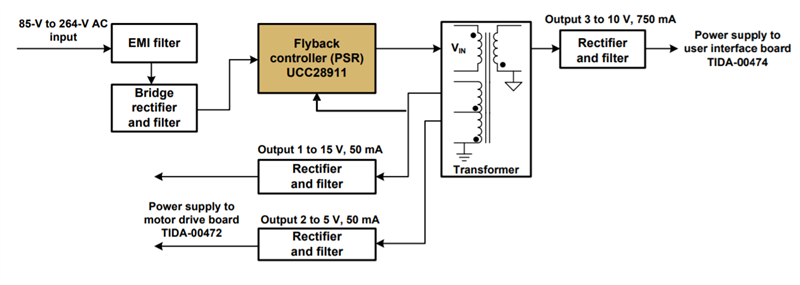 Figure 2 System block diagram of the 10-W bias supply reference design
The TLV733P is a low-dropout voltage regulator (LDO), with a a typical dropout of 125 mV at a 300-mA load and available in 1.0-V, to 3.3-V fixed output options. The TLV733P is stable without the need of input/output capacitors and is available in both the X2SON and SOT-23 packages, making it a great solution for space-constrained designs. Figure 3 shows a simplified schematic diagram of the TLV733P.
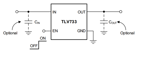 Figure 3 Simplified schematic diagram of the TLV33P
The TPS7A03 low-dropout regulator shown in Figure 4 is an ultra-low quiescent current device designed for power-sensitive applications. In addition to offering a quiescent current of 200-nA, the TPS7A03 also delivers an excellent transient response for always-on systems with dynamic loads. The quiescent current is virtually constant over the complete load current and ambient temperature range. The TPS7A03 serves as a great power-management attachment to low-power microcontrollers (MCUs) like the MSP430™ MCU. The TPS7A03 operates over an operating input voltage of 1.5 V to 6.0 V. It’s a good fit for both battery-powered systems as well as industrial applications that experience large line and load transients.
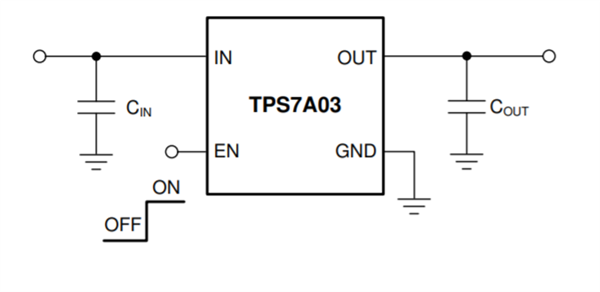 Figure 4 Simplified schematic diagram of the TPS7A03
Charging scheme
For a UV sterilization box, it’s important to shorten the charging time and extend the battery operation time. Figure 5 shows the 1.5-A integrated BQ25619 charging management and system power path management device, which can help meet both priorities. Its wide 3.9-V to 13.5-V input voltage range makes the BQ25619 a good fit for a variety of applications. The conduction resistor of the battery field-effect transistor is 19.5 mΩ, and the low-impedance power path management can help optimize the operation efficiency, shorten battery charging times and extend battery operation times in the discharge stage. With its 5-V input and 1-A charging current, charging efficiency can reach 94%. The I2C interface with charging and system settings makes it a flexible solution because designers can change the charging profile through I2C instead of external settings.
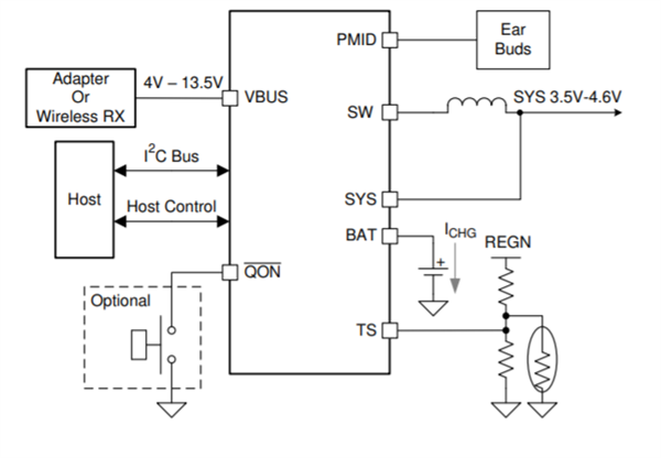 Figure 5 Simplified schematic diagram of the BQ25619
The BQ25616 shown in Figure 6 is a stand-alone battery charge management device with a maximum charging current of 3 A and a faster charging speed than the BQ25619 due to a higher charging current.
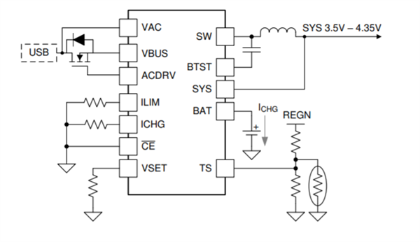 Figure 6 Simplified schematic diagram of the BQ25616
One particular design challenge in UV sterilization boxes is keeping the battery pack small in order to save room in the box. The BQ2970, shown in Figure 7, provides protection functions for single-cell lithium-ion/lithium-polymer battery packs, and monitors an external power MOSFET to provide protection in case of high charge and discharge currents, including overcharge protection, overdischarge protection, overcurrent protection and short-circuit detection. The current consumed in normal mode operation is 4 µA, reducing the battery’s power consumption. The size is 1.5 mm by 1.5 mm by 0.75 mm, which helps reduce the size of the battery pack.
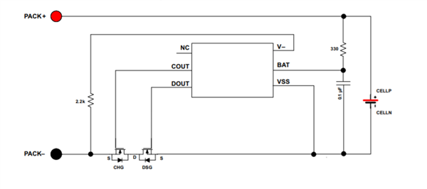 Figure 7 Simplified schematic diagram of the BQ2970
LED drive scheme
A high-performance red-green-blue LED driver is essential in smart home and other applications that include human interactions. Flicking, breathing and chasing LED animation effects can greatly improve the user experience by offering aesthetically pleasing visuals. Minimizing system noise is also crucial in these applications. The LP5012 (shown in Figure 8) is a 12-channel constant-current sink LED driver. This device includes integrated color mixing and brightness control, while pre-configuration features can help simplify the software coding process. The integrated 12-bit, 29-kHz pulse-width modulation (PWM) generator equipped for each channel can make LED colors smooth and vivid, and eliminate audible noise. Each LED is controlled independently, which helps achieve a smooth dimming effect. Independent color mixing and brightness control registers simplify software coding.
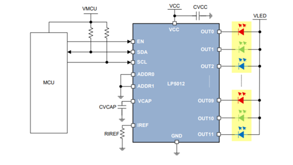 Figure 8 Simplified schematic diagram of the LP5012
The TPS61169 shown in Figure 9 is a boost LED driver with an integrated internal MOSFET that can drive LED strings in the UVC wavelength (between 200 and 280 nm). The LED current is set through the external sensor resistance, RSET. During operation, a PWM signal applied to the CTRL pin can control the LED current. The duty cycle of the PWM signal determines the feedback reference voltage. The TPS61169 will not burst LED current, so it does not generate audible noise on the output capacitor.
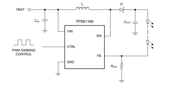 Figure 9 Simplified schematic diagram of the TPS61169
Master control scheme
The MSP430FR211x, shown in Figure 10,-is an ultra-low-power, low-cost MCU that has a powerful 16-bit reduced instruction set computer central processing unit, providing 2 KB to 4 KB of ferroelectric random access memory and 1 KB of static random access memory. The serial interface options include universal asynchronous receiver transmitter, Infrared Data Association or Serial Peripheral Interface; the MCU integrates a 6-bit digital-to-analog converter and an eight-channel 10-bit analog-to-digital converter and has 12 general-purpose input/output ports. Its low power consumption and quad flat no-lead 3-mm-by-3-mm packaging make it suitable for portable devices.
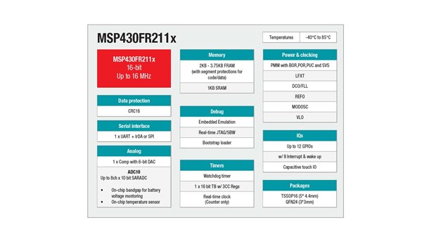 Figure 10 Internal resources of the MSP430FR211x
Audio scheme
An audio amplifier is used in a UV sterilization box in order for status indication. The TPA6203A1, shown in Figure 11, is a 1.25-W mono fully differential audio amplifier with a power-supply range of 2.5 V to 5.5 V, which can drive a speaker with an impedance of at least 8 Ω. The quiescent supply current is 1.7 mA, while shutdown mode consumes 10 µA. Its 2-mm-by-2-mm packaging with five peripheral devices conserves printed circuit board area.
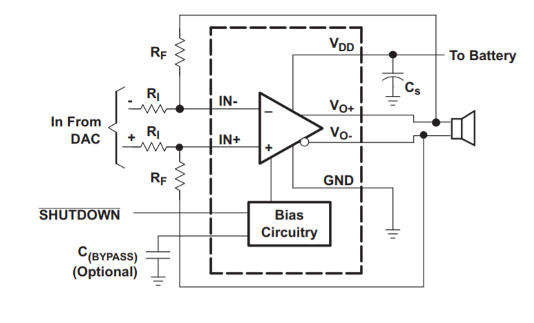 Figure 11 Reference schematic diagram of the TPA6203A1
To see a design using the TPA6203A1, check out the Reference Design for Automotive Cluster Driver Notification Functions.
TI has technologies that can help solve common design challenges when designing UV sterilization boxes, enabling designers to achieve benefits such as reduced system size, power savings and a pleasing user experience.