-
Migration Between TMS320F28002x and TMS320F28003x SPRUIW4 October 2021 TMS320F280021 , TMS320F280021-Q1 , TMS320F280023 , TMS320F280023-Q1 , TMS320F280023C , TMS320F280025 , TMS320F280025-Q1 , TMS320F280025C , TMS320F280025C-Q1 , TMS320F280033 , TMS320F280034 , TMS320F280034-Q1 , TMS320F280036-Q1 , TMS320F280036C-Q1 , TMS320F280037 , TMS320F280037-Q1 , TMS320F280037C , TMS320F280037C-Q1 , TMS320F280038-Q1 , TMS320F280038C-Q1 , TMS320F280039 , TMS320F280039-Q1 , TMS320F280039C , TMS320F280039C-Q1
-
Migration Between TMS320F28002x and TMS320F28003x
- Trademarks
- 1Feature Differences Between F28002x and F28003x
- 2PCB Hardware Changes
- 3Feature Differences for System Consideration
- 4Application Code Migration From F28002x to F28003x
- 5Specific Use Cases Related to F28003x New Features
- 6EABI Support
- 7References
- IMPORTANT NOTICE
Migration Between TMS320F28002x and TMS320F28003x
Trademarks
C2000 is a trademark of Texas Instruments.
All trademarks are the property of their respective owners.
1 Feature Differences Between F28002x and F28003x
F28003x is a superset of F28002x. They have three packages in common, 48-pin, 64-pin and 80-pin. It is possible to migrate between F28003x and F28002x with the caveats in this document taken into account.
1.1 F28002x and F28003x Feature Comparison
An overlaid block diagram of F28002x and F28003x is shown in Figure 1-1 while feature comparison of the superset part numbers for the F28003x and F28002x devices is shown in Table 1-1.
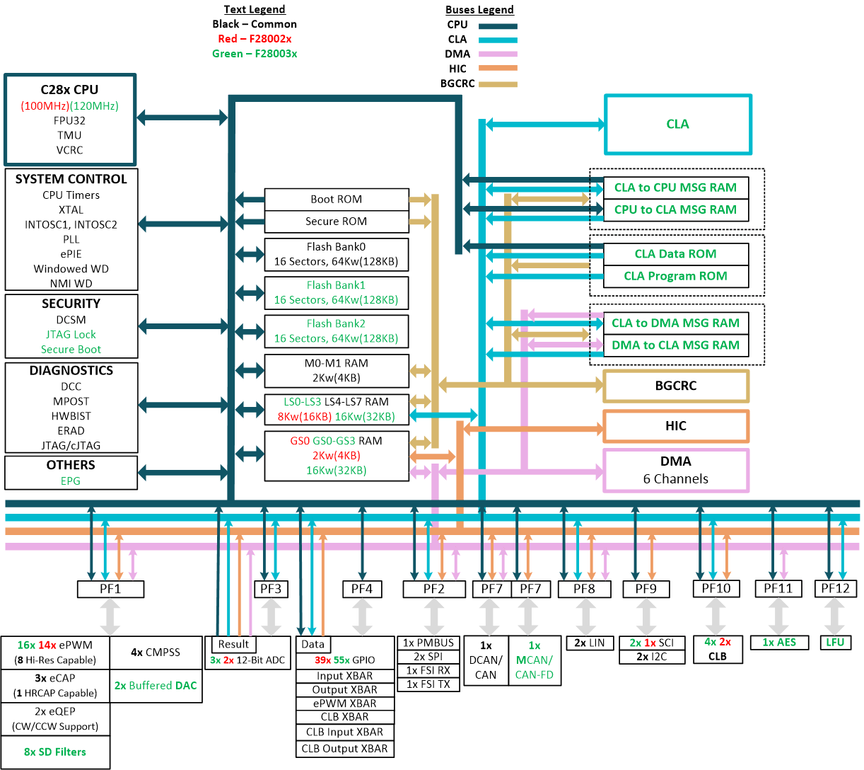 Figure 1-1 F28003x and F28002x Overlaid
Functional Block Diagram
Figure 1-1 F28003x and F28002x Overlaid
Functional Block Diagram| Feature | F28002x | F28003x | ||||||
|---|---|---|---|---|---|---|---|---|
| 80-Pin PN | 64-Pin PM | 48-Pin PT | 100-Pin PZ | 80-Pin PN | 64-Pin PM | 48-Pin PT | ||
| Processor and Accelerators | ||||||||
| C28x | Frequency (MHz) | 100 | 120 | |||||
| FPU | Yes (instructions for Fast Integer Division) | |||||||
| VCRC | Yes | |||||||
| TMU | Yes – Type 1 (instructions supporting NLPID) | |||||||
| CLA – Type 2 | Available | No | Yes | |||||
| Frequency (MHz) | - | 120 | ||||||
| 6–Channel DMA – Type 0 | Yes | |||||||
| External interrupts | 5 | |||||||
| Memory | ||||||||
| Flash | 128KB (64Kw) | 384KB (192Kw) | ||||||
| RAM | Dedicated | 4KB (2Kw) | ||||||
| Local Shared | 16KB (8Kw) | 32KB (16Kw) | ||||||
| Message | - | 1KB (0.5Kw) | ||||||
| Global Shared | 4KB (2Kw) | 32KB (16Kw) | ||||||
| Total | 24KB (12Kw) | 69KB (34.5Kw) | ||||||
| Message RAM Types | - | 512B (256w) CPU–CLA 512B (256w) CLA–DMA | ||||||
| ECC | FLASH, Mx, LSx | FLASH, Mx, LSx, GSx, Message RAM | ||||||
| Parity | GSx, ROM | ROM, CAN RAM | ||||||
| Code security for on–chip flash and RAM | Yes | |||||||
| System | ||||||||
| Configurable Logic Block (CLB) | 2 Tiles | 4 Tiles | ||||||
| Embedded Pattern Generator (EPG) | - | Yes | ||||||
| Motor Control Libraries in ROM | Yes | |||||||
| 32–bit CPU timers | 3 | |||||||
| Advance Encryption Standard (AES) | – | Yes | ||||||
| Background CRC (BGCRC) | Yes | |||||||
| Live Firmware Update (LFU) Support | – | Yes, with enhancements and flash bank erase time improvements | ||||||
| Secure Boot | – | Yes | ||||||
| JTAG Lock | – | Yes | ||||||
| HWBIST | Yes | |||||||
| Nonmaskable Interrupt Watchdog (NMIWD) timers | 1 | |||||||
| Watchdog timers | 1 | |||||||
| Crystal oscillator/External clock input | 1 | |||||||
| Internal oscillator | 2 | |||||||
| Pins and Power Supply | ||||||||
| Internal 3.3v to 1.2v Voltage Regulator | VREG LDO | Yes | ||||||
| GPIO pins | 39 | 26 | 14 | 51 | 39 | 26 | 14 | |
| Additional GPIO | 4 (2 from cJTAG and 2 from X1/X2) | |||||||
| AIO (analog with digital inputs) | 16 | 16 | 14 | 23 | 16 | 16 | 14 | |
| AGPIO (analog with digital inputs and outputs) | - | 2 | 2 | - | - | |||
| Analog Peripherals | ||||||||
| ADC 12–bit | Number of ADCs | 2 | 3 | |||||
| MSPS | 3.45 | 4 | ||||||
| Conversion Time (ns) | 290 | 250 | ||||||
| ADC channels (single–ended) - includes the two gpdac outputs on F28003x | 16 | 16 | 14 | 23 | 18 | 16 | 14 | |
| Temperature sensor | 1 | |||||||
| Buffered DAC | - | 2 | ||||||
| CMPSS (each CMPSS has two comparators and two internal DACs) | 4 | |||||||
| Control Peripherals | ||||||||
| eCAP/HRCAP modules | 3 (1 with HRCAP capability) – Type 2 | |||||||
| ePWM/HRPWM channels – Type 4 | 14 (8 with HRPWM) | 16 (8 with HRPWM) | ||||||
| eQEP modules | 2 – Type 2 | |||||||
| SDFM channels | - | 8 – Type 2 | ||||||
| Communication Peripherals | ||||||||
| CAN (DCAN) – Type 0 | 1 | |||||||
| CANFD (MCAN) – Type 1 | – | 1 | ||||||
| FSI | 1 (1 RX and 1 TX) – Type 1 | 1 (1 RX and 1 TX) – Type 2 | ||||||
| I2C – Type 1 | 2 | |||||||
| LIN – Type 1 | 2 | |||||||
| HIC | Yes - Type 0 | Yes - Type 1 | ||||||
| PMBus – Type 0 | 1 | |||||||
| SCI – Type 0 | 1 | 2 | ||||||
| SPI – Type 2 | 2 | |||||||
| Package Options, Temperature, and Qualification | ||||||||
| Junction temperature (TJ) | –40°C to 125°C | –40°C to 150°C | ||||||
| Free-Air temperature (TA) | –40°C to 125°C | |||||||
| Package Options with AEC-Q100 Qualification available | Yes | Yes | Yes | Yes | – | Yes | Yes | |
2 PCB Hardware Changes
The F28002x and F28003x devices have three packages in common: 80-pin PN, 64-pin PM and 48-pin PT. The following sections describe the pin migration in detail.
2.1 PCB Hardware Changes for the 80-Pin PN, 64-Pin PM and 48-Pin PT Packages
This section describes the F28003x and F28002x differences that exist between the 80-Pin PN, 64-Pin PM and 48-Pin PT packages.
80-Pin PN: The Q and non-Q variant for F28002x have the same pinout whereas F28003x has no Q variant for 80-Pin PN. Figure 2-1 outlines the differences.
64-Pin PM: The Q and non-Q variant for F28002x have the same pinout whereas VREGENZ replaces GPIO39 in the Q variant for F28003x. Figure 2-2 and Figure 2-3 outline the differences.
48-Pin PT: The Q and non-Q variant have the same pinout for both devices. Figure 2-4 outlines the differences.
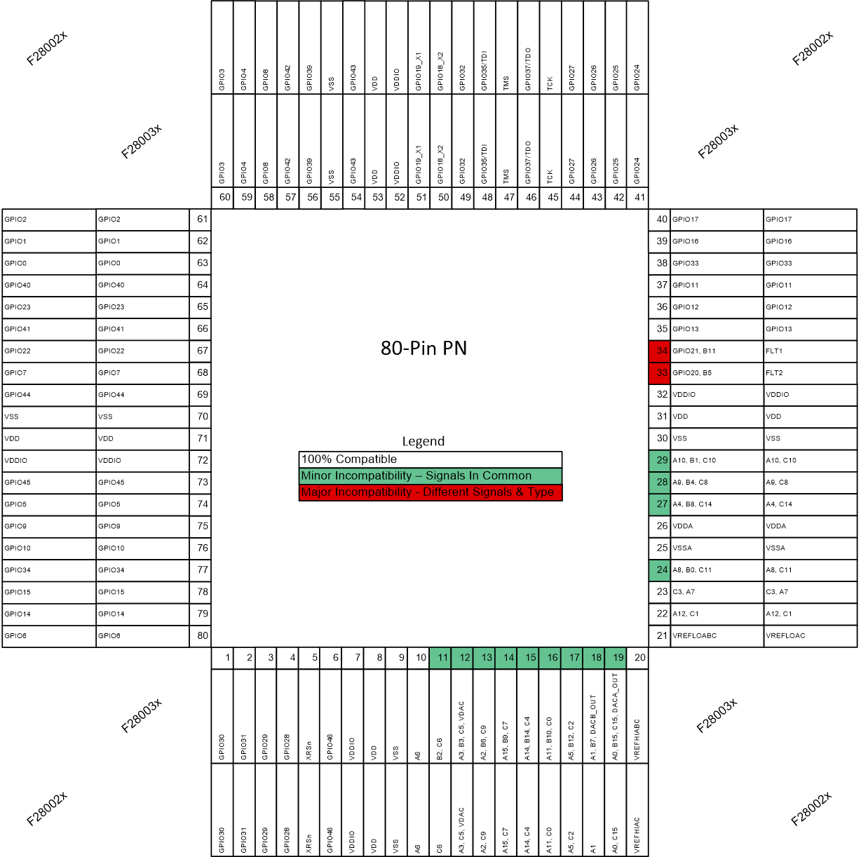 Figure 2-1 80-Pin PN, F28003x and F28002x
Pin-Overlay
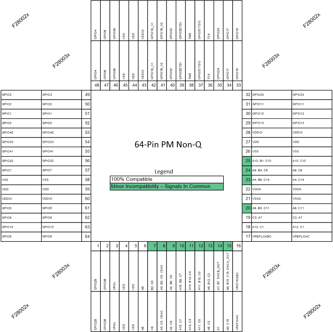 Figure 2-2 64-Pin PM Non-Q Variant, F28003x and
F28002x Pin-Overlay
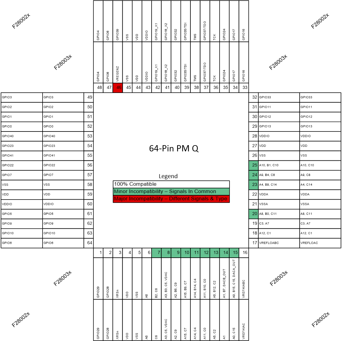 Figure 2-3 64-Pin PM Q Variant, F28003x and
F28002x Pin-Overlay
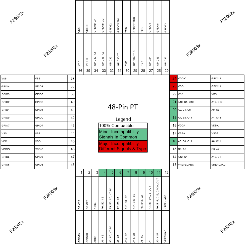 Figure 2-4 48-Pin PT, F28003x and F28002x
Pin-Overlay
Figure 2-4 48-Pin PT, F28003x and F28002x
Pin-Overlay2.2 80-Pin PN, 64-Pin PM and 48-Pin PT Migration Between F28002x and F28003x For New and Existing PCB
For the color legend, see Figure 2-1 through Figure 2-4.
| Pin No | Pin Name | Transition Type | Action | ||||
|---|---|---|---|---|---|---|---|
| 80 | 64 | 48 | F28002x | F28003x | F28003x to F28002x | F28002x to F28003x | |
| Minor Incompatibility - Signals in Common (1) | |||||||
| 10 | 6 | 4 | A6 | A6 | Common Analog Channel | Use A6 (No change for 64-Pin and 80-Pin) | |
| 11 | 7 | C6 | B2, C6 | Use C6 | |||
| 12 | 8 | 5 | A3, C5, VDAC | A3, B3, C5 VDAC | Use A3, C5 or VDAC | ||
| 13 | 9 | 6 | A2, C9 | A2, B6, C9 | Use A2 or C9 | ||
| 14 | 10 | 7 | A15, C7 | A15, B9, C7 | Use A15 or C7 | ||
| 15 | 11 | - | A14, C4 | A14, B14, C4 | Use A14 or C4 | ||
| 16 | 12 | 8 | A11, C0 | A11, B10, C0 | Use A11 or C0 | ||
| 17 | 13 | 9 | A5, C2 | A5, B12, C2 | Use A5 or C2 | ||
| 18 | 14 | 10 | A1 | A1, B7, DACB_OUT | Use A1 | ||
| 19 | 15 | 11 | A0, C15 | A0, B15, C15, DACA_OUT | Use A0 or C15 | ||
| 24 | 20 | 16 | A8, C11 | A8, B0, C11 | Use A8 or C11 | ||
| 27 | 23 | 19 | A4, C14 | A4, B8, C14 | Use A4 or C14 | ||
| 28 | 24 | 20 | A9, C8 | A9, B4, C8 | Use A9 or C8 | ||
| 29 | 25 | 21 | A10, C10 | A10, B1, C10 | Use A10 or C10 | ||
| Major Incompatibility - Different Signals and Types | |||||||
| 33 | - | - | FLT2 | GPIO20, B5 | Flash Test Pins to GPIO/Analog | No connect. Enable internal pull-up for the GPIOs on F28003x | |
| 34 | - | - | FLT1 | GPIO21, B11 | |||
| - | - | 23 | GPIO13 | VDD | Power to GPIO | Tie to VDD through 0-Ohm resistor. Depopulate resistor when using F28002x and enable internal pull-up for the GPIO | |
| - | - | 24 | GPIO12 | VDDIO | Tie to VDDIO through 0-Ohm resistor. Depopulate resistor when using F28002x and enable internal pull-up for the GPIO | ||
| (Q Variant) Major Incompatibility - Different Signals and Types | |||||||
| - | 46 | - | GPIO39 | VREGENZ | External VREG not supported. Tie to VSS through 0-Ohm resistor. Depopulate resistor when using F28002x and enable internal pull-up for the GPIO | ||
3 Feature Differences for System Consideration
The differences and similarities that exist when moving between the F28003x and F28002x devices is explored in this section.
3.1 New Features in F28003x
This section outlines features that only exist in the F28003x device. For details on each of these new features, see the TMS320F28003x Real-Time Microcontrollers Technical Reference Manual (SPRUIW9).
3.1.1 Advance Encryption Standard (AES)
The AES module on F28003x is a symmetric cipher module that provides hardware-accelerated data encryption and decryption with support for 128-, 192- and 256-bit keys. AES was first introduced in F2838x.
3.1.2 Secure Boot/JTAG Lock
The F28003x device supports secure booting and also has the capability to lock the JTAG to avoid debug access thereby enhancing security. Secure Boot and JTAG Lock were first introduced in F2838x.
3.1.3 Modular Controller Area Network (MCAN)
The MCAN module on F28003x supports CAN FD (CAN with the flexible data-rate) specification which has a higher throughput compared to Classic CAN. It can also operate in Classic CAN mode if needed. MCAN was first introduced in F2838x.
3.1.4 Embedded Pattern Generator (EPG)
The EPG on F28003x is an interface module that can be used to generate waveforms and clocks for other modules on the device. This can be useful for communication module diagnostics and also providing the modulation clock for the SDFM.
3.1.5 Live Firmware Update (LFU)
The F28003x device has in-built hardware to facilitate live firmware updates. It supports fast context switching from the old firmware to the new firmware to minimize application downtime when updating the device firmware.
3.2 Communication Module Changes
Communication module changes between the F28002x and F28003x devices affect the number of modules, addition of CAN-FD and some differences in HIC and FSI. Details are available in Table 3-1.
| Module | Category | F28002x | F28003x | Notes |
|---|---|---|---|---|
| LIN | Number | 2 - LINA, LINB | 2 - LINA, LINB | |
| CAN | Number | 1- CANA | 1- CANA | |
| CAN-FD | Number | not present | 1 - MCANA | |
| SCI | Number | 1 - SCIA | 2 - SCIA, SCIB | |
| SPI | Number | 2 - SPIA, SPIB | 2 - SPIA, SPIB | |
| I2C | Number | 2 -I2CA, I2CB | 2 -I2CA, I2CB | |
| PMBUS | Number | 1 - PMBUSA | 1 - PMBUSA | |
| FSI | Number | 1 - FSIA | 1 - FSIA | |
| Register | - | TX_OPER_CTRL_LO.SEL_TDM_IN | Transmit TDM Mode Enable bit | |
| - | TX_DLYLINE_CTRL | Transmit delay line control register | ||
| - | RX_MASTER_CTRL.DATA_FILTER_EN | Data filter enable bit | ||
| - | RX_TRIG_CTRL_0 | Receive Trigger Control register 0 | ||
| - | RX_TRIG_WIDTH_0 | Receive Trigger Wdith register 0 | ||
| - | RX_TRIG_CTRL_1 | Receive Trigger Control register 1 | ||
| - | RX_TRIG_CTRL_2 | Receive Trigger Control register 2 | ||
| - | RX_TRIG_CTRL_3 | Receive Trigger Control register 3 | ||
| - | RX_UDATA_FILTER | Receive User Data Filter Control register | ||
| HIC | Number | 1 - HICA | 1 - HICA | |
| Register | - | HICCOMMIT | Commit bit for the HICLOCK register |
3.3 Control Module Changes
There are minimal changes in the control modules between the F28002x and F28003x devices. The biggest change is the addition of an SDFM module for the F28003x device. Table 3-2 shows the module instances differences which should be considered when migrating applications between F28002x and F28003x.
| Module | Category | F28002x | F28003x | Notes |
|---|---|---|---|---|
| SDFM | Number | - | 8 - SD1_D1C1..D4C4, SD2_D1C1..D4C4 | |
| eQEP | Number | 2 - EQEP1, EQEP2 | ||
| eCAP | Number | 3 - ECAP1..3 | ||
| HRCAP | Number | 1 - HRCAP3 | ||
| ePWM | Number | 7 - EPWM1..7 | 8 - EPWM1..8 | Blanking window improvements on F28003x |
| Registers | DCFCTL.PULSESEL | DCFCTL.PULSESEL | Blank Pulse Mix added as an option for F28003x | |
| HRPWM | Number | 4 - HRPWM1..4 | ||