-
Designing With the C2000™ Embedded Pattern Generator (EPG) SPRACY7 October 2021 TMS320F2800132 , TMS320F2800133 , TMS320F2800135 , TMS320F2800137 , TMS320F2800152-Q1 , TMS320F2800153-Q1 , TMS320F2800154-Q1 , TMS320F2800155 , TMS320F2800155-Q1 , TMS320F2800156-Q1 , TMS320F2800157 , TMS320F2800157-Q1 , TMS320F280033 , TMS320F280034 , TMS320F280034-Q1 , TMS320F280036-Q1 , TMS320F280036C-Q1 , TMS320F280037 , TMS320F280037-Q1 , TMS320F280037C , TMS320F280037C-Q1 , TMS320F280038-Q1 , TMS320F280038C-Q1 , TMS320F280039 , TMS320F280039-Q1 , TMS320F280039C , TMS320F280039C-Q1
-
Designing With the C2000™ Embedded Pattern Generator (EPG)
Designing With the C2000™ Embedded Pattern Generator (EPG)
Trademarks
C2000 is a trademark of Texas Instruments.
All trademarks are the property of their respective owners.
1 Introduction
The Embedded Pattern Generator (EPG) module is a customizable pattern and clock generator that could serve many test and application scenarios that require a simple pattern generator or a periodic clock generator. The EPG module can also be used to capture an incoming serial stream of data. The EPG module allows users to design new clock generators,pulse width modulators (PWMs), serial communication modules, and so forth.
The EPG module can be used as an independent peripheral or it can be used along side other peripherals such as CAN. When used alongside other peripherals, such as CAN, EPG can provide signal patterns for testing and running diagnostic inside the C2000™ device.
1.1 Supplementary Information
For more information on the EPG module on a specific C2000 device, see the device-specific data sheet and the corresponding Technical Reference Manual (TRM).
This application report was written using the TMS320F28003x family of devices. The data sheet and TRM used for this application report are listed below:
- TMS320F28003x Real-Time Controllers Technical Reference Manual
- TMS320F28003x Real-Time Microcontrollers
Additional support is provided by the TI E2E™ Community.
2 Clock Generator
The EPG can be used to generate clock signals. These clock signals can be used internally by the EPG (the EPG SIGGENx modules), or be exported out of the EPG through EPGOUTx signals. If exported out of the EPG through the EPGOUTx signals, then these clock signals can be used by other peripherals through the XBARs (EPGOUTs are connected to Output XBAR and CLB Output XBAR for F28003x) or be sent out of the device through GPIOs.
For example, for F28003x, EPG1 EPGOUT0 and EPGOUT1 are connected to Output XBAR. Therefore, EPGOUT0 and EPGOUT1 can be sent out of the device through GPIOs configured for Output XBAR. Also, on F28003x, the EPG1 EPGOUT2 and EPGOUT3 are connected to CLB Output XBAR, therefore; they can also be sent out of the device through GPIOs.
The EPG CLKGEN modules generate two version of output signals. The DCLK outputs are approximately 50% duty while the GCLK are the gated clocks. DCLKs can be exported out of the EPG module through EPGOUTx signals. GCLKs are used by the SIGGEN modules inside the EPG.
2.1 Generating Two Offset Clocks
Each CLKGEN module can generate four GCLK and four DCLK outputs. Each of the four output clocks have their own OFFSET. All clocks within the same CLKGEN module share the same clock divider counter (CLKDIVx_CTL0.PRD).
To generate two offset clocks based on EPGCLK, there is no need for an external input to the EPG. That means the EPGIN signals are not used and, therefore, no configuration of the Input XBAR is needed. In the F28003x device, EPG1 EPGIN1 to EPGIN4 are sourced from Input XBAR INPUT13 to INPUT16, but in this example, those resources from Input XBAR can be used for other purposes.
To generate the two offset clock signals, CLKGEN0 of EPG1 is used. CLKGEN0 of EPG1 will generate CLKOUT0_DCLK as the reference clock signal, and CLKOUT1_DCLK as the offset clock signal.
The EPGOUT0 and EPGOUT1 MUXes must configured to output:
- EPGOUT0: CLKGEN0 → CLKOUT0_DCLK
- EPGOUT1: CLKGEN0 → CLKOUT1_DCLK
This is show in Figure 2-1.
Next, CLKGEN0 must be configured to divide the EPGCLK down using CLDIV0_CTL0.PRD and create offsets by configuring the CLKDIV0_CLKOFFSET.CLK0OFFSET and CLKDIV0_CLKOFFSET.CLK1OFFSET. In this example EPGCLK is divided by 100, and the two CLKOUT0 and CLKOUT1 are offset by 25.
- CLDIV0_CTL0.PRD = 100 - 1
- CLKDIV0_CLKOFFSET.CLK0OFFSET = 0
- CLKDIV0_CLKOFFSET.CLK1OFFSET = 25
To output EPGOUT0 and EPGOUT1 to GPIOs, Output XBAR must be used. Two Output XBAR OUTPUTs must be configured to select the EPGOUT0 and EPGOUT1 signals, and the device PinMux must be configured to use Output XBAR on the corresponding GPIOs.
For F28003x, SYSCLK is set to 120 MHz. With a clock divider of 100, the frequency of the generated CLKOUT0_DCLK and CLKOUT1_DCLK are 1.2 MHz. The clock offset of 25 for CLKOUT1_DCLK, offsets the signal from CLKOUT0_DCLK by 200 ns.
If the SIGGEN0 module is configured for any mode other than BIT-BANG mode, the clock generation will stop until the SIGGEN0 module starts a ROTATE or SHIFT. Therefore, inserting the line below will disable the clock generation in this example.
EPG_setSignalGenMode(EPG1_BASE, EPG_SIGGEN0, EPG_SIGGEN_MODE_SHIFT_RIGHT_ONCE);C2000Ware example 7 showcases this example configuration.
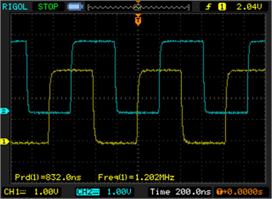 Figure 2-2 Two Offset Clocks
3 Signal Generator
EPG signal generators (SIGGENx) modules can generate or capture complex digital patterns. SIGGENx modules can be configured to many different modes (rotate right mode, shift right mode, and so forth).
SIGGENx modules are clocked from the CLKGENx modules. Therefore, the CLKGENx modules must be configured.
A simple pattern that can be generated by a SIGGEN module is same pattern as the two offset clocks examples previously generated by the CLKGEN module.
3.1 Two Offset Clocks Generated by the SIGGEN0 Module
To generate the same offset clock signals as before using the SIGGEN0 module, the CLKGEN module (which will be clocking SIGGEN0) will be different from the previous example.
The first step is to configure the CLKGEN0 module to generate a clock which will be used by the SIGGEN0 module. To start let's generate CLKGEN0 CLKOUT0 to be EPGCLK divided by 10:
- Setting the CLKDIV0 PRD to be 10 - 1
In the last example with the two offset clocks generated by the CLKGEN0 module, the generated clocks were 100 times slower than EPG clock. So far in this example, the CLKDIV0 has divided EPG clock by a factor of 10. The other divide by 10 will be handled inside the SIGGEN0 module.
The output of the SIGGEN0 module must then be used to drive the EPGOUT0 and EPGOUT1. In this example we will use DATATRANOUT0 and DATATRANOUT2 for EPGOUT0 and EPGOUT1.
To configure the SIGGEN module for generating our offset clock output signals, the following settings are used:
- BIT-BANG mode is NOT used.
- BIT LENGTH of the SIGGEN module is set to 10. This is our DIVIDE 10 for the signal generator, which alongside the CLKDIV0 PRD will generate the EPGCLK/100 output signal frequency. Having a BIT LENGTH of 10, and a CLKDIV PRD of 10 will restrict our output signal offset resolution to be EPGCLK/10.
- Since BIT LENGTH of 10 means that you specify a 10-bit serial stream. For 50% duty cycle of the output signal, the 10 bit serial data is set to "0b0000011111". Each bit in the 10-bit stream will be an (EPGCLK Period)x10 long HIGH/LOW level in the output signal.
- The data to SIGGEN0_DATA0 and SIGGEN0_DATA1 is written by you.
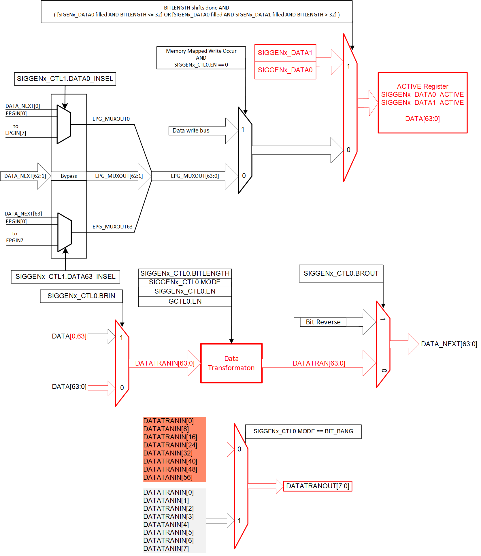 Figure 3-2 SIGGEN0 Configuration
Generating Two Offset Clocks
Figure 3-2 SIGGEN0 Configuration
Generating Two Offset ClocksSince BIT-BANG mode is not used:
- DATATRANOUT0 ← DATATRANIN0
- DATATRANOUT1 ← DATATRANIN8
- DATATRANOUT2 ← DATATRANIN16
- DATATRANOUT3 ← DATATRANIN24
Currently, DATATRANOUT0 will be used to output DATATRANIN0 for EPGOUT0. For EPGOUT1, DATATRANOUT2 (connected to DATATRANIN16) is used. Since out BIT-LENGTH is set to 10 (10-bit stream), DATATRANOUT1 (connected to DATATRANIN8) is NOT used.
- DATATRANIN0 to DATATRANIN15 used
for the first output (only the first 10 bits are used).DATATRANIN0 → DATATRANOUT0 → EPGOUT0
- DATATRANIN16 to DATATRANIN31 used
for the second output (only the first 10 bits are used).DATATRANIN16 → DATATRANOUT2 → EPGOUT1
Last the SIGGEN module is configure for ROTATE RIGHT REPEAT, to ensure that the data is CONTINUOUSLY generated.
The two 10-bit data streams are concatenated and written to SIGGEN0_DATA0:
- SIGGEN0_DATA0 = (0b0000011111) | ((0b0000011111 << CLOCK_OFFSETS) << 16)
CLOCK_OFFSET can be any value between ZERO and BIT-LENGTH. This will determine the offset between the two output signals. The 16-bit shift, places the second 10-bit stream in SIGGEN0_DATA0 [16:31] which will be tapped at bit 16 by DATATRANOUT2.
With a 10-bit stream, the second clock output cannot be shifted to exactly match the previous example. If the second serial stream is shifter by 2 bits (CLOCK_OFFSETS = 2), the output will be as shown in Figure 3-3.
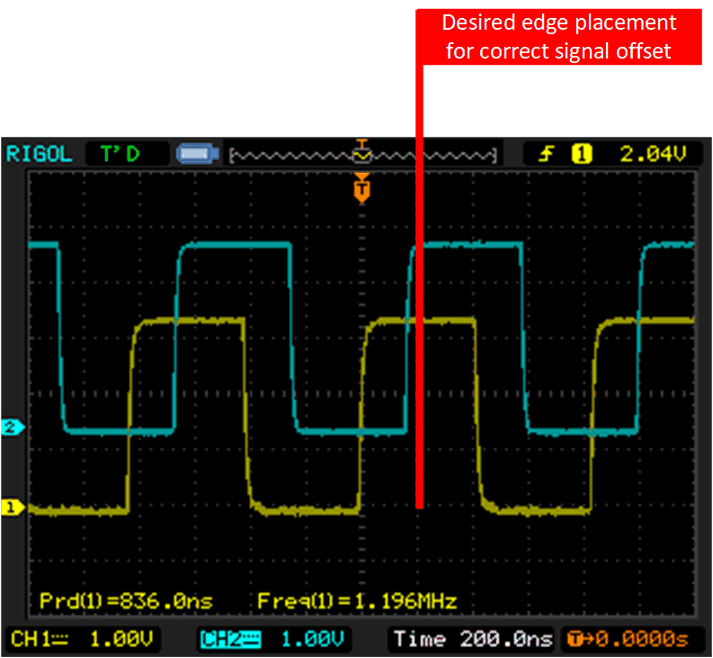 Figure 3-3 Generated Signal Offset -
Shift by 2
Figure 3-3 Generated Signal Offset -
Shift by 2If the second bit stream is shifted by 3 (CLOCK_OFFSET = 3), the output will be as shown in Figure 3-4.
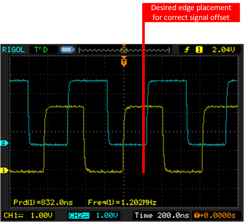 Figure 3-4 Generated Signal Offset -
Shift by 3
Figure 3-4 Generated Signal Offset -
Shift by 3Since you cannot shift by 2.5 bits, the divider settings must be changed. To perfectly match the signal from the previous example and offset the output signals by 200 ns (F28003x device clocking assumed), the clock divider in CLKDIV0 (CLKGEN0) must be set to 5 and the BIT-LENGTH of the SIGGEN module set to 20. This will ensure the same EPGCLK/100 setting, while allowing a twice higher resolution for the clock offset settings. If the 20-bit serial stream is shifted by 5, the output signals will perfectly match the ones from the previous example.
3.2 Generate Serial Data With Rotate Mode
The SIGGEN module can operate in ROTATE RIGHT ONCE mode. This mode can be used to generate both serial data and serial clock signals. This example will generate the serial clock and serial data signals, similar to the SPI module. The SPI clock and data signals can be generated in four possible modes.
 Figure 3-6 SPI Modes
All different modes of the SPICLK and SPI data can be generated by the EPG SIGGEN module. Table 3-1 maps the name of the SPICLK mode with the SPI clock polarity and phase modes.
| SPICLK Mode | SPI Clock Phase and Polarity |
|---|---|
| Rising edge without delay | CPOL=0, CPHA=0 |
| Rising edge with delay | CPOL=0, CPHA=1 |
| Falling edge without delay | CPOL=1, CPHA=0 |
| Falling edge with delay | CPOL=1, CPHA=1 |
Both the SPICLK and SPI data are generated by the SIGGEN module. The SIGGEN module will be clocked by the CLKGEN module. Similar to the previous example, the frequency of the SPICLK generated will depend on the CLKGEN period and the SIGGEN BIT-LENGTH. In this example, the CLKGEN period is set to 10 (meaning EPGCLK/10) and the BIT-LENGTH of the SIGGEN module is set 16.
With a BIT-LENGTH of 16, the SIGGEN module can generate SPICLK and SPI data signals which can output an 8-bit word on the GPIO. SIGGEN module requires a minimum BIT-LENGTH of 16 to be able place SPICLK edges between the generated SPI data. In this example, rotate right once mode is used. The same signals can be generated through the SHIFT RIGHT ONCE mode as well (explored in the next section).
3.2.1 Rotate Right Once - CPOL = 0, CPHA = 1
The SPI data serial bit stream is placed in SIGGEN0_DATA0[15:0], while the SPI clock serial bit stream is placed in SIGGEN0_DATA0[31:16]. SIGGEN0_DATA1 is not used in this mode.
The clock and data bit stream for CPOL=0 and CPHA=1 is shown below:
//
// Data
//
#define SIG_GEN_DATA0_0_15    0b1111000011001111U

//
// Clock - Data latched on rising edge, during idle CLK is LOW
//
#define SIG_GEN_DATA0_16_31   0b1010101010101010U
For the serial data bit stream, each TWO consecutive bits are the same. This allows 256 different patterns (8-bit data) to be generated. For the serial clock bit steam, the transition from 0 to 1 occurs during in between the serial data bit repetition.
In ROTATE RIGHT ONCE mode, the clock signal generated will begin with the LOW (0) state as soon as the SIGGEN module in enabled. After the 16 rotate operations are completed on the DATA[63:0] of the SIGGEN0 module, the SIGGEN0 module will reload the SIGGEN0_DATA0 and SIGGEN0_DATA1 registers into the active registers. This means that the IDLE state of the clock is LOW (0).
The idle state of the SIGGEN generated serial data is SIGGEN0_DATA0[0] and the idle state of generated serial clock is SIGGEN0_DATA0[16]. This means that the idle state of the clock signal will always be LOW, while the idle state of the data signal will depend on the data.
After a full BIT-LENGTH shift has been completed, the SIGGEN module is disabled. The user can fill in the new data in SIGGEN0_DATA0 and re-enable the SIGGEN module to generate new data. The EPG interrupt status flags can be checked to determine if the SIGGEN module has completed all operations, or to determine whether new data should be loaded into the SIGGEN module.
epg1_gintsts = EPG_getInterruptStatus(EPG1_BASE);
if (epg1_gintsts & EPG_INT_SIGGEN0_DONE){
    EPG_clearInterruptFlag(EPG1_BASE, epg1_gintsts);
    EPG_setData0Word(EPG1_BASE, EPG_SIGGEN0, (SIG_GEN_DATA0_0_15 | (uint32_t)SIG_GEN_DATA0_16_31 << 16));
    EPG_enableSignalGen(EPG1_BASE, EPG_SIGGEN0);
}
Interrupts can also be generated by the EPG module. For the F28003x, the EPG interrupt is the SYS_ERROR interrupt (INT_SYS_ERR).
3.2.2 Rotate Right Once - CPOL=0, CPHA=0
In order to generate the same data on the SPI data line as the previous example , this time with CPOL=0 and CPHA=0 mode signal format, the EPG SIGGEN DATA bit stream must be updated.
The clock and data bit stream for CPOL=0 and CPHA=0 is shown below.
//
// Data
//
#define SIG_GEN_DATA0_0_15    0b1110000110011111U

//
// Clock - Data latched on falling edge, during idle CLK is LOW
//
#define SIG_GEN_DATA0_16_31   0b1010101010101010U
In this mode, falling edges latch the data, and the data line must be delayed.
3.2.3 Rotate Right Once - CPOL=1, CPHA=1
The clock and data bit stream for CPOL=1 and CPHA=1 is shown below:
//
// Data
//
#define SIG_GEN_DATA0_0_15    0b1111000011001111U

//
// Clock - Data latched on falling edge, during idle CLK is HIGH
//
#define SIG_GEN_DATA0_16_31   0b0101010101010101U
The data bit stream in this mode is the same as CPOL=0, CPHA=1. The clock bit stream is inverted to place falling edges in between duplicated data stream bits.
 Figure 3-11 Rotate Right Once - CPOL=1,
CPHA=1
Figure 3-11 Rotate Right Once - CPOL=1,
CPHA=13.2.4 Rotate Right Once - CPOL=1, CPHA=0
The clock and data bit stream for CPOL=1 and CPHA=0 is shown below:
//
// Data
//
#define SIG_GEN_DATA0_0_15    0b1110000110011111U

//
// Clock - Data latched on rising edge, during idle CLK is HIGH
//
#define SIG_GEN_DATA0_16_31   0b0101010101010101U
The data bit stream in this mode is the same as CPOL=0, CPHA=0. The clock bit stream is inverted to place rising edges in between duplicated data stream bits.
 Figure 3-12 Rotate Right Once - CPOL=1,
CPHA=0
Figure 3-12 Rotate Right Once - CPOL=1,
CPHA=0Next, creating the same signals using the SIGGEN module in SHIFT RIGHT ONCE mode will be discussed.
3.2.5 Shift Right Once - CPOL=1, CPHA=0
In this example, the main difference between ROTATE right once mode and SHIFT right once mode is that after BIT-LENGHT shifts are done in SHIFT RIGHT ONCE mode, the SIGGEN0_DATA0 and SIGGEN0_DATA1 registers are NOT loaded into the active SIGGEN data. Therefore, when SHIFT RIGHT ONCE mode is used, after BIT-LENGTH shifts are done, the IDLE signal level of the data line will be the first bit in the clock stream. The IDLE signal level of the clock line will be the DATA[32] bit that corresponds to SIGGEN0_DATA1[0].
//
// Data
//
#define SIG_GEN_DATA0_0_15    0b1111000011001111U

//
// Clock - Data latched on rising edge
//
#define SIG_GEN_DATA0_16_31   0b1010101010101010U

//
// During idle CLK is HIGH
//
#define SIG_GEN_DATA1_0 0b1When the device PinMux is configured to be driven by Output X-Bar (which is sourced from EPGOUT), while the SIGGEN module is not enable, the signal output on the GPIO is LOW (0). When the SIGGEN module is enabled for the very first time, the generated SPI clock signal will be low until the first "1" in the clock bit stream.
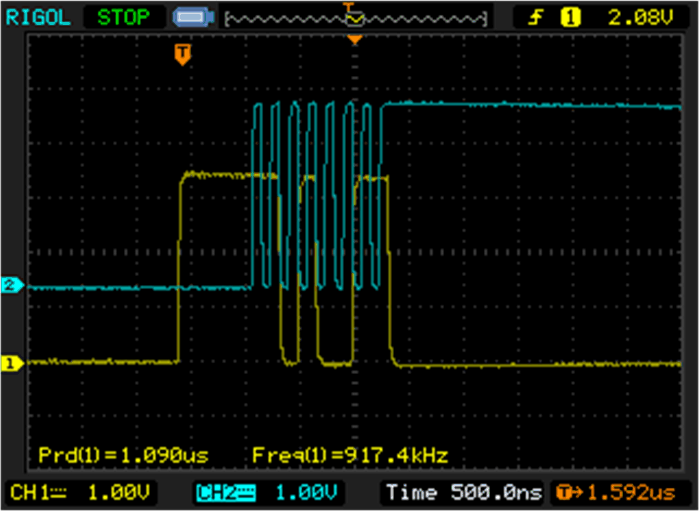 Figure 3-14 Shift Right Once First Data
and Clock Generation - CPOL=1, CPHA=0
Figure 3-14 Shift Right Once First Data
and Clock Generation - CPOL=1, CPHA=0As shown in Figure 3-14, the SPI clock generated is in the LOW state before the first data and clock pattern is generated. The clock signal IDLE state after the first pattern is generated is HIGH.
In all following transfers, the IDLE state of the clock before and after each pattern generation will always be HIGH.
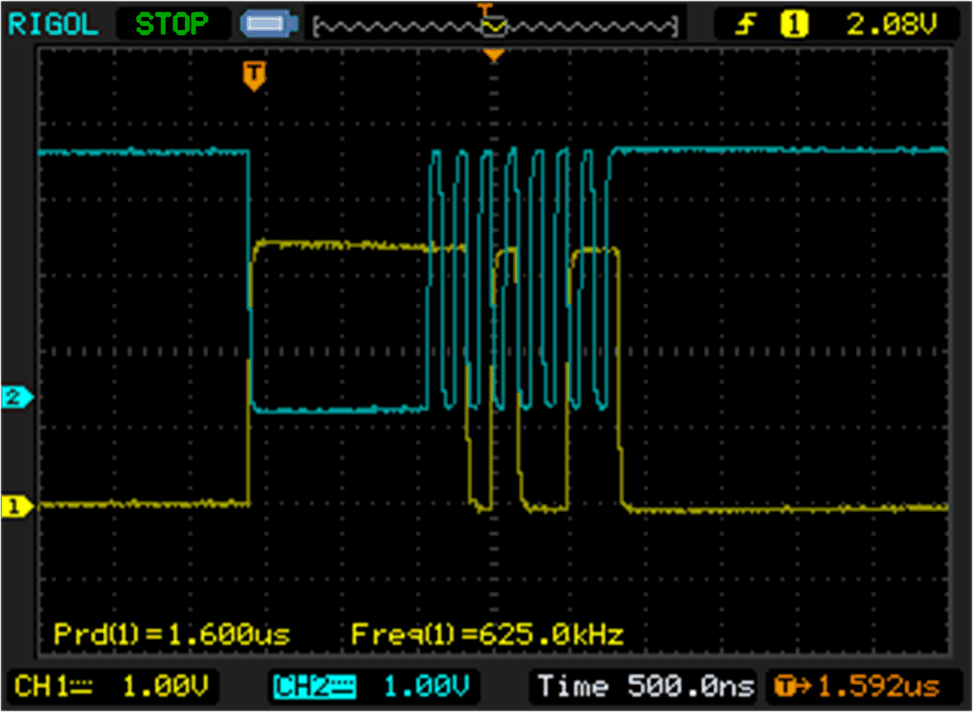 Figure 3-15 Shift Right Once All Other
Data and Clock Generation - CPOL=1, CPHA=0
Figure 3-15 Shift Right Once All Other
Data and Clock Generation - CPOL=1, CPHA=0A zoomed in view of the data and clock generated relevant to each other is shown in Figure 3-16.
3.2.6 Shift Right Once - CPOL=0, CPHA=0
In this example, once again the SHIFT right once mode is used, and the SIGGEN0_DATA0 and SIGGEN0_DATA1 registers are NOT loaded into the active SIGGEN data. Therefore, when SHIFT RIGHT ONCE mode is used, after BIT-LENGTH shifts are done, the IDLE signal level of the data line will be the first bit in the clock stream. The IDLE signal level of the clock line will be the DATA[32] bit which corresponds to SIGGEN0_DATA1[0].
//
// Data
//
#define SIG_GEN_DATA0_0_15    0b1111000011001111U

//
// Clock - Data latched on falling edge
//
#define SIG_GEN_DATA0_16_31   0b0101010101010101U

//
// During idle CLK is LOW
//
#define SIG_GEN_DATA1_0       0b0
When the device PinMux is configured to be driven by Output X-Bar (which is sourced from EPGOUT), while the SIGGEN module is not enable, the signal output on the GPIO is LOW (0). When the SIGGEN module is enabled for the very first time, the generated SPI clock signal will be low until the first "1" in the clock bit stream.
In all following transfers, the IDLE state of the clock before and after each pattern generation will always be LOW.
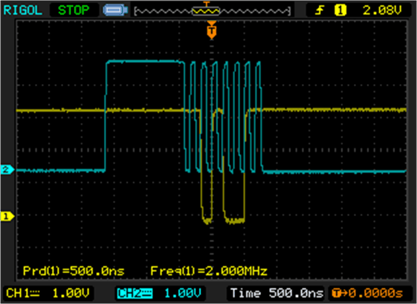 Figure 3-18 Shift Right Once All Other
Data and Clock Generation - CPOL=0, CPHA=0
Figure 3-18 Shift Right Once All Other
Data and Clock Generation - CPOL=0, CPHA=0A zoomed in view of the data and clock generated relevant to each other is shown in Figure 3-19.
As it can be seen in all of the examples above, using the SHIFT/ROTATE right modes requires the bit streams placed in SIGGEN registers to be changed. The IDLE state for the data and clock patterns depend on which mode is selected. If the SHIFT mode is selected, the data IDLE state depends on the first bit of the clock bit stream. The user can configure the SIGGEN module to have a BIT-LENGTH of 17 to decouple the data signal's IDLE state bit from the clock bit stream's first bit.
4 Summary
The Embedded Pattern Generator (EPG) module is a powerful and highly customizable pattern and clock generator that could serve many test and application scenarios that require a simple pattern generator or a periodic clock generator. The EPG module can be used to create an additional serial communication, pulse width modulator, or some other peripheral inside a C2000 device.
5 References
- Texas Instruments: TMS320F28003x Real-Time Controllers Technical Reference Manual
- Texas Instruments: TMS320F28003x Real-Time Microcontrollers
IMPORTANT NOTICE AND DISCLAIMER
| TI PROVIDES TECHNICAL AND RELIABILITY DATA (INCLUDING DATASHEETS), DESIGN RESOURCES (INCLUDING REFERENCE DESIGNS), APPLICATION OR OTHER DESIGN ADVICE, WEB TOOLS, SAFETY INFORMATION, AND OTHER RESOURCES “AS IS” AND WITH ALL FAULTS, AND DISCLAIMS ALL WARRANTIES, EXPRESS AND IMPLIED, INCLUDING WITHOUT LIMITATION ANY IMPLIED WARRANTIES OF MERCHANTABILITY, FITNESS FOR A PARTICULAR PURPOSE OR NON-INFRINGEMENT OF THIRD PARTY INTELLECTUAL PROPERTY RIGHTS. |
| These resources are intended for skilled developers designing with TI products. You are solely responsible for (1) selecting the appropriate TI products for your application, (2) designing, validating and testing your application, and (3) ensuring your application meets applicable standards, and any other safety, security, or other requirements. These resources are subject to change without notice. TI grants you permission to use these resources only for development of an application that uses the TI products described in the resource. Other reproduction and display of these resources is prohibited. No license is granted to any other TI intellectual property right or to any third party intellectual property right. TI disclaims responsibility for, and you will fully indemnify TI and its representatives against, any claims, damages, costs, losses, and liabilities arising out of your use of these resources. |
| TI’s products are provided subject to TI’s Terms of Sale (www.ti.com/legal/termsofsale.html) or other applicable terms available either on ti.com or provided in conjunction with such TI products. TI’s provision of these resources does not expand or otherwise alter TI’s applicable warranties or warranty disclaimers for TI products. |
| Mailing Address: Texas Instruments, Post Office Box 655303, Dallas, Texas 75265
Copyright © 2021, Texas Instruments Incorporated |