-
Achieve Delayed Protection for Three-Level Inverter With CLB SPRACY3 June 2021 F29H850TU , F29H859TU-Q1 , TMS320F280023C , TMS320F280025C , TMS320F280025C-Q1 , TMS320F280040C-Q1 , TMS320F280041C , TMS320F280041C-Q1 , TMS320F280048C-Q1 , TMS320F280049C , TMS320F280049C-Q1 , TMS320F28076 , TMS320F28379D , TMS320F28379D-Q1 , TMS320F28379S , TMS320F28386D , TMS320F28386D-Q1 , TMS320F28386S , TMS320F28386S-Q1 , TMS320F28388D , TMS320F28388S , TMS320F28P650DH , TMS320F28P650DK , TMS320F28P650SH , TMS320F28P650SK , TMS320F28P659DH-Q1 , TMS320F28P659DK-Q1 , TMS320F28P659SH-Q1
-
Achieve Delayed Protection for Three-Level Inverter With CLB
Achieve Delayed Protection for Three-Level Inverter With CLB
Trademarks
C2000 is a trademark of Texas Instruments Incorporated.
All trademarks are the property of their respective owners.
1 Introduction
Nowadays, three-level inverter topology has become increasingly popular in high power applications, like UPS and solar inverter. By increasing the bus voltage to 1000-V or 1500-V DC, the current can be reduced to maintain the same power levels, which can significantly reduce the power loss with less copper design. Besides, three-level inverter topology makes it possible to use the same switching device to support this much higher voltage stress than before. However, compared with traditional two-level inverter, in addition to more complicated power conversion control, a different fault protection scheme is required for three-level inverter.
Figure 1-1 shows a typical single phase three-level I-Type inverter, named neutral point clamped (NPC) inverter. The single phase NPC inverter includes 4 FETs, like IGBT, in series, where S1 and S4 are called outer switches, with S2 and S3 called inner switches.
 Figure 1-1 Single Phase Three-Level I-Type
Inverter
Figure 1-1 Single Phase Three-Level I-Type
InverterThe based control of the four series FETs are as follows.
- S1 always switches opposite of S3, and S4 always switches opposite of S2. There is a dead time between S1 and S3, as well as between S4 and S2, which always prevents a shoot-through condition.
- S1 and S4 cannot be on simultaneously.
Considering the difference between positive cycle and negative cycle when tied to the grid, the general switching states of 4 FETs in normal operation are shown in Table 1-1.
| Symbol | Switching States | |||
|---|---|---|---|---|
| S1 | S2 | S3 | S4 | |
| Positive | Alternate switch | Remaining ON | Alternate switch | Remaining OFF |
| Negative | Remaining OFF | Alternate switch | Remaining ON | Alternate switch |
There are several events which lead to quick shut-down to protect the semiconductors and the system, like over current, thermal overload, and so forth. Unlike immediately switching off all the FETs simultaneously in two level inverter, for three-level inverter, it must be made sure that the correct switch-off sequence is maintained: outer switches (S1 or S4) off first, inner switches (S2 or S3) off after a specific delay, while the inner one must be switched on firstly during the recover process. This delayed protection requirement has been a challenge for lots of UPS or solar inverter customers for a long time. Since using software algorithm will cause too much delay to provide in-time protection, some customers have to use external hardware circuits, like FPGA or CPLD, to achieve such protection logic, which increases the system cost and also the development effort.
The C2000 configurable logic block (CLB) is a collection of configurable blocks that interconnect through software to implement custom digital logic functions, which can be an option to replace the function achieved by external CPLD or FPGA. This application report has designed and validated a simple protection scheme with CLB, and also discussed several extra requirements in three-level inverter. The example code is based on F280049C, and it can be easily migrated to any other C2000 devices with CLB, including F28388D/S, F28386D/S, F28379D/S, F28076 and F28004xC.
2 Design Overview
Figure 2-1 shows the expected EPWM protection results with CLB during positive cycle and negative operation.
In the given example, EPWM1A/2B/1B/2A are used for S1/2/3/4 control, respectively. The trip signal is simulated and generated with an EPWM output, EPWM8A here, for the validation of different trip conditions, including trip sustaining within or across one EPWM cycle.
Taking positive cycle operation as example, shown in 'A' of Figure 2-1, whenever the trip event occurs, EPWM1A and EPWM1B, which are configured with cycle-by-cycle tripping (CBC) action, are shut down immediately, while EPWM2B will be forced low after a delay t2. Besides, when the trip event disappears, EPWM2B will turn high immediately, which is also aligned with the basic recover requirement. The CLB signal is the key internal signal for the delayed trip feature, and EPWM1B and EPWM2B are actually the result of the AND logic of the initial EPWM output (EPWM1B’ and EPWM2B’) and CLB signal.
3 CLB Implementation
3.1 CLB Input Selection
EPWM1B and EPWM2B are routed to CLB TILE1 and TILE2, respectively, before outputting as external signals. Taking EPWM1B as example, it is routed to CLB1 by Global Signal Bus via Input Mux of Tile 1. The trip signal, sourced from the specific GPIO, needs to take 2 input bits, to form the predefined logic later.
To import these three signals into the CLB (BOUNDARY INz, where z is any number between 0–7) from the GPIOs, INPUT X-BAR and CLB X-BAR configurations are needed.
    // Configure CLB-XBAR AUXSIG0 as INPUTXBAR1
    //
    XBAR_setCLBMuxConfig(XBAR_AUXSIG0, XBAR_CLB_MUX01_INPUTXBAR1);
    XBAR_enableCLBMux(XBAR_AUXSIG0, XBAR_MUX01);

// CLB tile 1 configuration
    CLB_configLocalInputMux(CLB1_BASE, CLB_IN0, CLB_LOCAL_IN_MUX_GLOBAL_IN);
    CLB_configLocalInputMux(CLB1_BASE, CLB_IN1, CLB_LOCAL_IN_MUX_GLOBAL_IN);
    CLB_configLocalInputMux(CLB1_BASE, CLB_IN2, CLB_LOCAL_IN_MUX_GLOBAL_IN);

    CLB_configGlobalInputMux(CLB1_BASE, CLB_IN0, CLB_GLOBAL_IN_MUX_CLB_AUXSIG0);
    CLB_configGlobalInputMux(CLB1_BASE, CLB_IN1, CLB_GLOBAL_IN_MUX_CLB_AUXSIG0);
    CLB_configGlobalInputMux(CLB1_BASE, CLB_IN2, CLB_GLOBAL_IN_MUX_EPWM1B);

    CLB_configGPInputMux(CLB1_BASE, CLB_IN0, CLB_GP_IN_MUX_EXTERNAL);
    CLB_configGPInputMux(CLB1_BASE, CLB_IN1, CLB_GP_IN_MUX_EXTERNAL);
    CLB_configGPInputMux(CLB1_BASE, CLB_IN2, CLB_GP_IN_MUX_EXTERNAL);
The above code snippet shows the input configuration for EPWM1B. In this example, INPUT X-BAR 1 is used to route the trip signal from GPIO, and CLB X-BAR enables INPUT X-BAR 1 as the source for AUXSIG0, according to the CLB X-BAR Mux Configuration Table in the TRM. Here the trip signal is assigned for both CLB Input 0 and CLB Input 1. That is because the rising edge of the trip signal is needed to determine the rise edge of the expected CLB signal, which will be discussed later, so the input filter selection feature is used to detect the rising edge of the trip signal.
CLB_selectInputFilter(CLB1_BASE, CLB_IN1, CLB_FILTER_RISING_EDGE);3.2 Counter and FSM Configuration
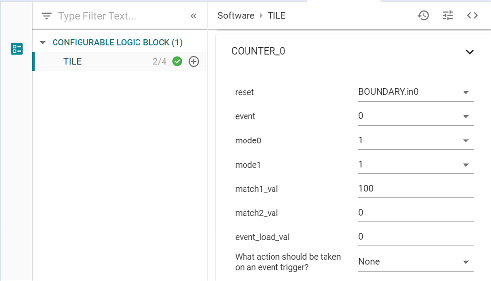
The counter block is used to achieve the customized delay. Since the counter will always reset to 0 if the “Reset” input remains high, the trip signal, which is active low, can be used to trigger the counter to start counting. Thus, both MODE_0 and MODE_1 can be set to 1, which enables the counter increment as soon as the trip signal goes low. MATCH1 is set with the expected delay value, like 100, which means 1 μs, with the time base of 100 MHz for CLB module. Figure 3-1 shows how the counter is configured in the GUI-based SysConfig tool.
 Figure 3-1 Counter Settings in the
SysConfig
Figure 3-1 Counter Settings in the
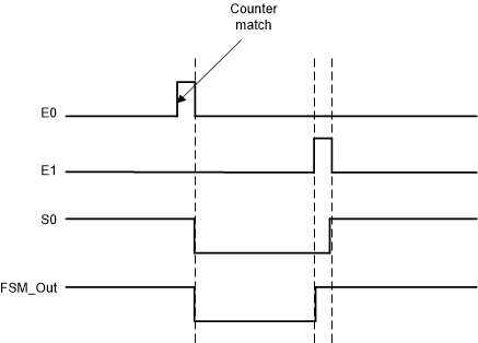
SysConfigThe state machine has been implemented with the FSW block as shown in Figure 3-2. Two inputs are used to identify the state of S0. E0 is referred to the counter match event, while E1 is the rising edge of the trip signal. Thus, S0 will go down at E0 and rise at E1. Thus, the Karnaugh map can be created for S0 state, as given in Table 3-1.
 Figure 3-2 State Machine in the FSW
Block
Figure 3-2 State Machine in the FSW
Block| S0 | E0E1 | 00 | 01 | 11 | 10 |
|---|---|---|---|---|---|
| 0 | 0 | 1 | 1 | 0 | |
| 1 | 1 | 1 | 0 | 0 |
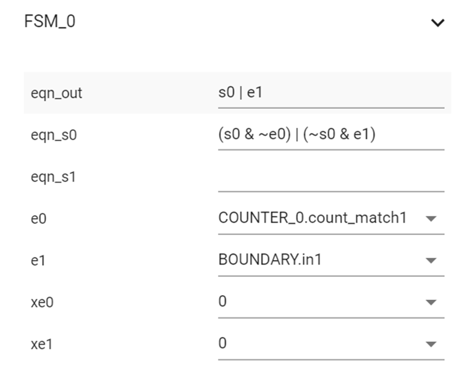
Based on the Karnaugh map, the FSM equations for S0 can be deduced as shown in Equation 1.
Since the state transitions will always take 1 clock cycle to take effect, in order to reduce the undesirable delay, the FSM output takes the combinational output of S0 and E1, that is shown in Equation 2.
 Figure 3-3 FSM Configuration
3.3 CLB Output
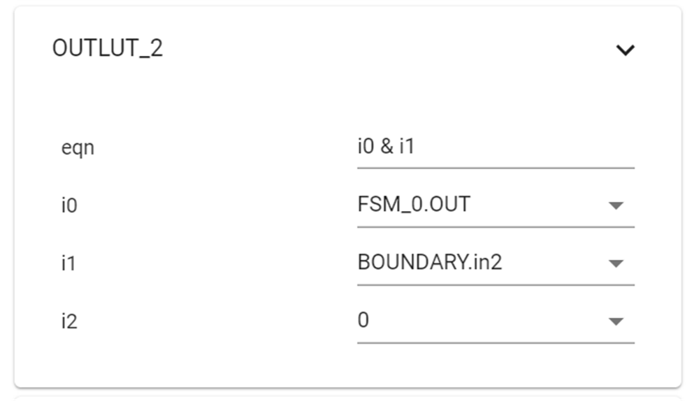
The final step is to use the output LUT block to combine the FSM_OUT and original EPWM1B’ with AND logic. According to the Table 3-2, OUTPUT LUT2_0 of CLB TILE1 is used to route the resulting output (FSM_OUT&EPWM1B’) as the new EPWM1B, as shown in Figure 3-4. Likewise, OUTPUT LUT2_0 of CLB TILE2 is used for EPWM2B. That is why two CLB TILEs are required in this application.
| CLB Instance | CLB Output Signal | Peripheral Signal | Peripheral Name |
|---|---|---|---|
| CBL1 | CLB1_OUT0_0 | PWMA | EPWM1 |
| CBL1 | CLB1_OUT1_0 | PWMA_OE | EPWM1 |
| CBL1 | CLB1_OUT2_0 | PWMB | EPWM1 |
| CBL1 | CLB1_OUT3_0 | PWMB_OE | EPWM1 |
| CBL1 | CLB1_OUT4_0 | AQ_PWMA | EPWM1 |
| CBL1 | CLB1_OUT5_0 | AQ_PWMB | EPWM1 |
| CBL1 | CLB1_OUT6_0 | DB_PWMA | EPWM1 |
| CBL1 | CLB1_OUT7_0 | DB_PWMB | EPWM1 |
| CBL1 | CLB1_OUT0_1 | QA | EQEP1 |
| CBL1 | CLB1_OUT1_1 | QB | EQEP1 |
| CBL1 | CLB1_OUT2_1 | DDIR | EQEP1 |
| CBL1 | CLB1_OUT3_1 | QCLK | EQEP1 |
| CBL1 | CLB1_OUT4_1 | G1.2 | CLB X BAR |
| CBL1 | CLB1_OUT5_1 | G3.2 | CLB X BAR |
 Figure 3-4 OUTPUT LUT2_0 Configuration
 As shown in Table 3-2, each CLB output signal passes through an external multiplexer that intersects a specific peripheral signal. Thus, to export the CLB output to the original EPWM1B pin (GPIO1 in the example), it is needed to enable the OUTPUT LUT2_0 using the OUT_EN register, as shown in the below code snippets.
CLB_setOutputMask(CLB1_BASE, 0x4, true);   //1<<2 out2

CLB_setOutputMask(CLB2_BASE, 0x4, true);  //1<<2 out2
3.4 Completed Design
One of the tools provided with CCS is the graphical Tile Viewer showing all CLB components and the associated signal interconnections for a given CLB design. Figure 3-5 shows the completed block diagram of the design, including the logic connections among FSM, LUT and the Counter, with logic equations.
 Figure 3-5 Completed Design Block
Diagrams
Figure 3-5 Completed Design Block
DiagramsIn addition, as shown in the block diagram, the “BOUNDARY” items are added as the tile inputs to simulate the CLB function before the test. As shown in Figure 3-5, both “in0” and “in1” are defined as a same periodic PWM referring to the trip signal, where the rising edge is selected for the “in-edge” option of “in1”. “in2” is set as 1, which represents normally high EPWM1B or EPWM2B.
 Figure 3-6 Boundary Input Setting
Once the CLB configuration and input stimuli have been defined, the simulation results can be obtained with the GTKwave viewer, as shown in Figure 3-7. And the expected delayed action is achieved at the CLB output signal. Note that the “clock_period” of the Global Parameters in the .syscfg tool should be changed to 10 ns, in order to match the time base of 100 MHz for CLB module, as shown in Figure 3-8. For more details of the CLB simulator, see the CLB Tool User's Guide.
 Figure 3-7 CLB Simulation Result
 Figure 3-8 Global Parameters
Configuration