SNVSB03D December   2018  – January 2020

PRODUCTION DATA.  

  1. Features
  2. Applications
  3. Description
    1.     Device Images
      1.      Typical Application Circuit
      2.      TPS3840 Typical Supply Current
  4. Revision History
  5. Device Comparison
  6. Pin Configuration and Functions
    1.     Pin Functions
  7. Specifications
    1. 7.1 Absolute Maximum Ratings
    2. 7.2 ESD Ratings
    3. 7.3 Recommended Operating Conditions
    4. 7.4 Thermal Information
    5. 7.5 Electrical Characteristics
    6. 7.6 Timing Requirements
    7. 7.7 Typical Characteristics
  8. Detailed Description
    1. 8.1 Overview
    2. 8.2 Functional Block Diagram
    3. 8.3 Feature Description
      1. 8.3.1 Input Voltage (VDD)
        1. 8.3.1.1 VDD Hysteresis
        2. 8.3.1.2 VDD Transient Immunity
      2. 8.3.2 User-Programmable Reset Time Delay
      3. 8.3.3 Manual Reset (MR) Input
      4. 8.3.4 Output Logic
        1. 8.3.4.1 RESET Output, Active-Low
        2. 8.3.4.2 RESET Output, Active-High
    4. 8.4 Device Functional Modes
      1. 8.4.1 Normal Operation (VDD > VDD(min))
      2. 8.4.2 VDD Between VPOR and VDD(min)
      3. 8.4.3 Below Power-On-Reset (VDD < VPOR)
  9. Application and Implementation
    1. 9.1 Application Information
    2. 9.2 Typical Application
      1. 9.2.1 Design 1: Dual Rail Monitoring with Power-Up Sequencing
        1. 9.2.1.1 Design Requirements
        2. 9.2.1.2 Detailed Design Procedure
        3. 9.2.1.3 Application Curves
      2. 9.2.2 Design 2: Battery Voltage and Temperature Monitor
        1. 9.2.2.1 Design Requirements
        2. 9.2.2.2 Detailed Design Procedure
      3. 9.2.3 Design 3: Fast Start Undervoltage Supervisor with Level-shifted Input
        1. 9.2.3.1 Design Requirements
        2. 9.2.3.2 Detailed Design Procedure
      4. 9.2.4 Design 4: Voltage Monitor with Back-up Battery Switchover
        1. 9.2.4.1 Design Requirements
        2. 9.2.4.2 Detailed Design Procedure
      5. 9.2.5 Application Curve: TPS3840EVM
  10. 10Power Supply Recommendations
  11. 11Layout
    1. 11.1 Layout Guidelines
    2. 11.2 Layout Example
  12. 12Device and Documentation Support
    1. 12.1 Device Nomenclature
    2. 12.2 Support Resources
    3. 12.3 Trademarks
    4. 12.4 Electrostatic Discharge Caution
    5. 12.5 Glossary
  13. 13Mechanical, Packaging, and Orderable Information
Device Comparison

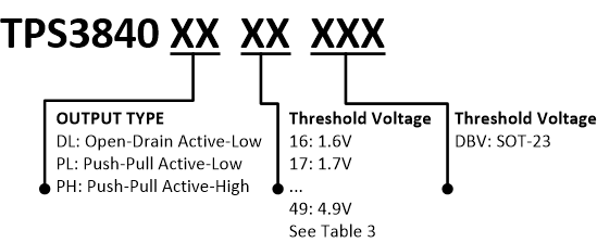
Figure 1 shows the device nomenclature to determine the device variant. Other voltages from Table 3 at the end of datasheet can be sample upon request, please contact TI sales representative for details.

TPS3840 TPS3840_device_nomenclature.gifFigure 1. Device Nomenclature