SNVAA19 May 2021 LP8863-Q1 , LP8864-Q1 , LP8864S-Q1 , LP8866-Q1 , LP8866S-Q1
4 Boost OVP Design Consideration
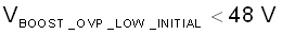
When the voltage of DISCHARGE pin is higher than VBOOST_OVPH (typically 50 V, minimum 48.5 V for LP8866-Q1), boost OVP high fault will be reported and device will go to fault recovery until boost voltage falls below threshold before restarting, as shown in Table 3-1. Be careful when designing boost OVP low threshold of initial voltage considering the overshoot during start-up. The boost OVP low threshold of initial voltage should be designed to be triggered first before DISCHARGE pin reaching VBOOST_OVPH. Otherwise, boost OVP high fault will be reported if DISCHARGE pin reaches 48.5 V during start-up. Then the device will go to fault recovery mode and restart again and again. Therefore, we recommend to design VBOOST_OVP_LOW_INITIAL < 48 V, as shown in Equation 4.
Where:
- VBOOST_OVP_LOW_INITIAL is the boost OVP Llow threshold for initial voltage during start up
- 48 V is 0.5 V (additional margin) below the minimum VBOOST_OVPH.