SNLU254A November 2020 – July 2022 DS160PT801
5 DS160PT801X16EVM Schematic
Figure 5-1 through Figure 5-2 illustrate the DS160PT801X16EVM schematics.
Figure 5-1 Schematic – Cover Sheet
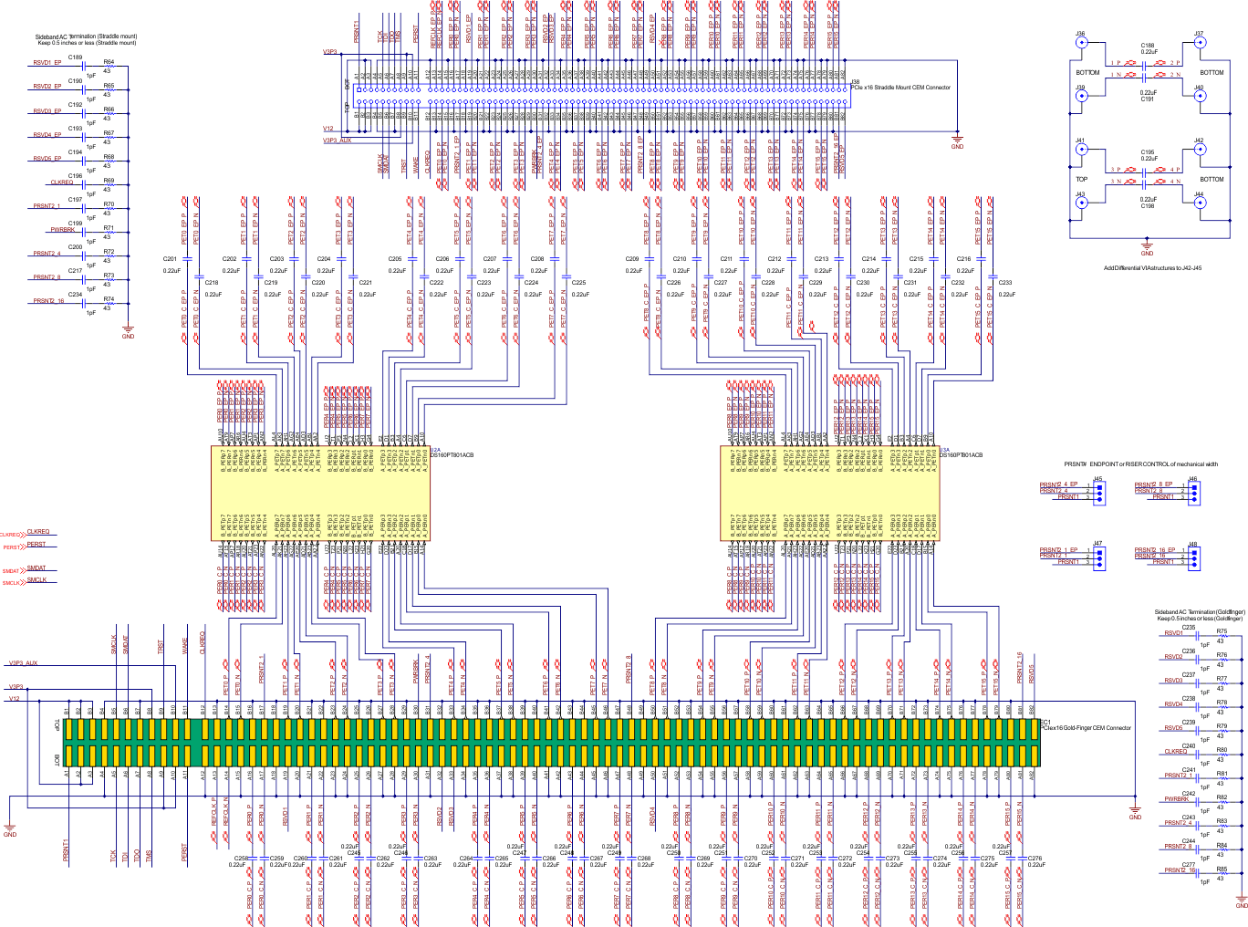 Figure 5-2 Schematic – High Speed
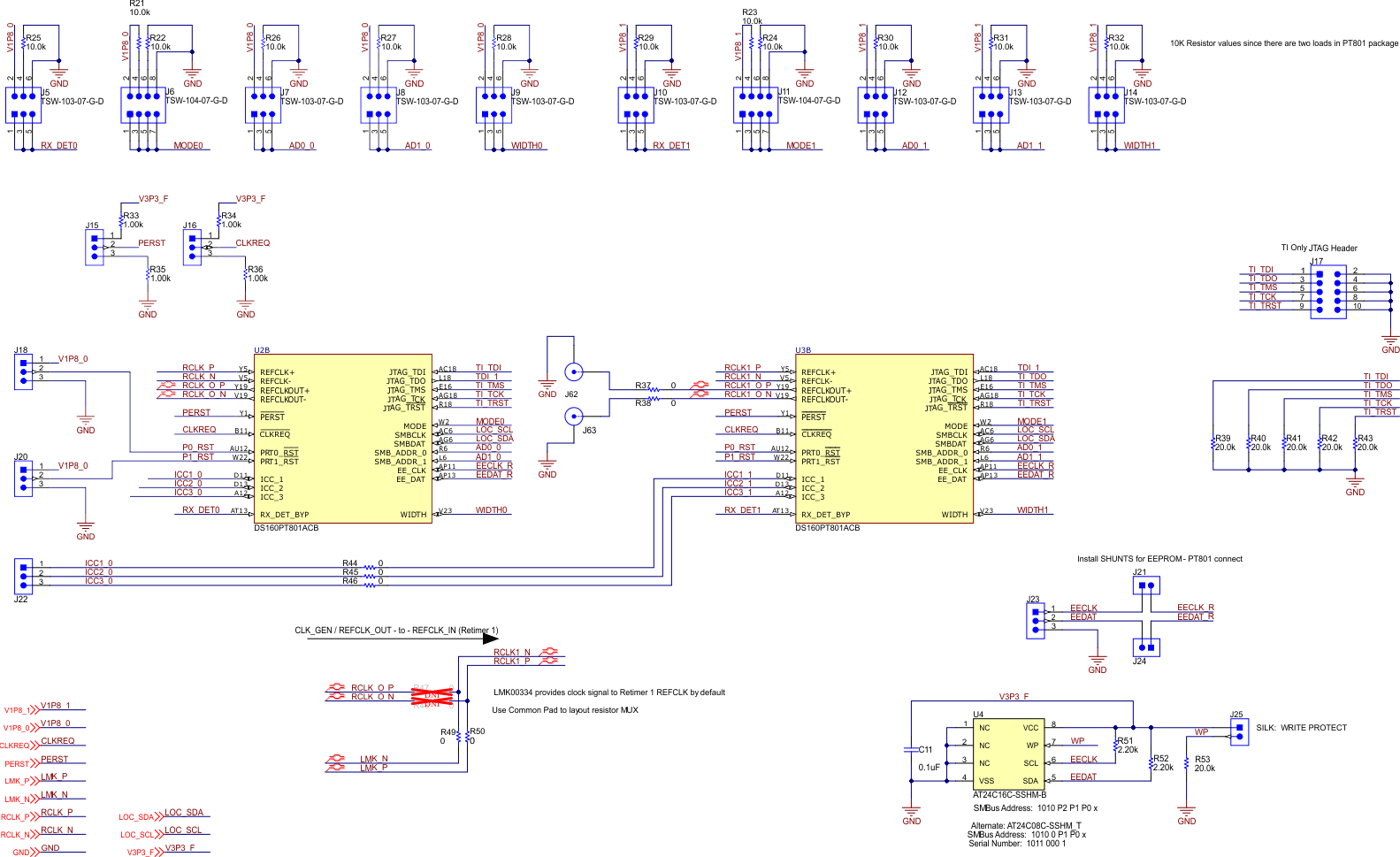 Figure 5-3 Schematic – Control
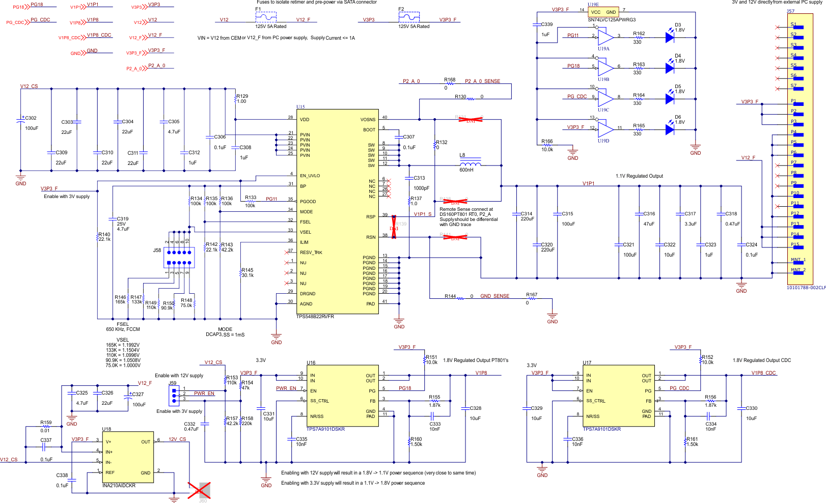 Figure 5-4 Schematic – Supply Voltage
Regulators
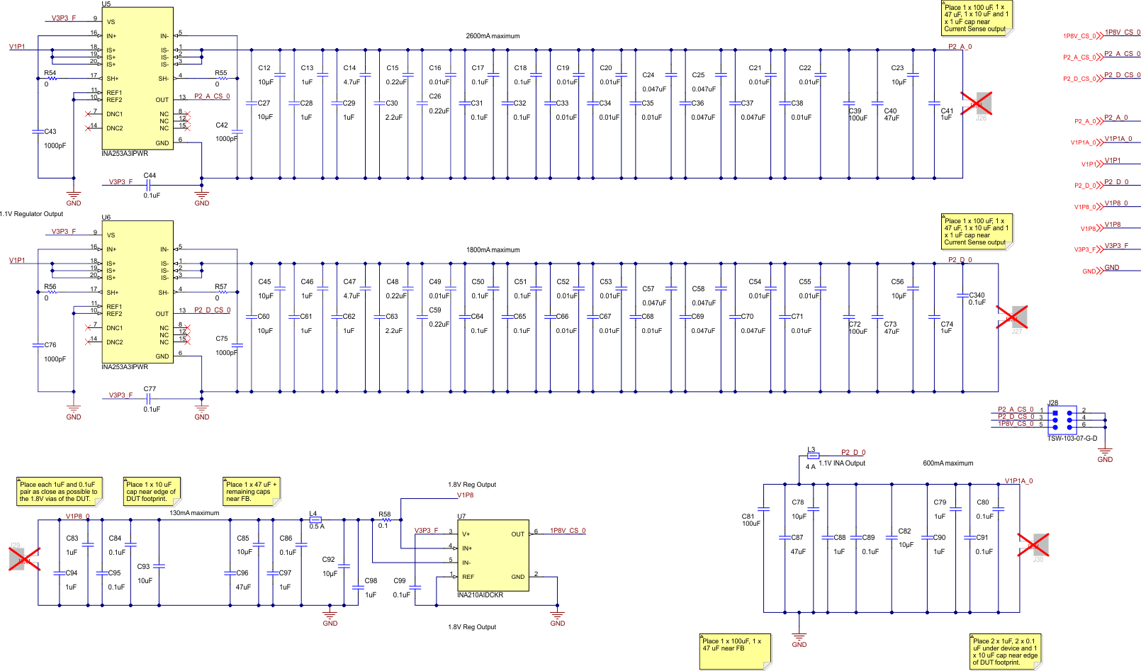 Figure 5-5 Schematic – Retimer 1 Current Sense
and Decoupling
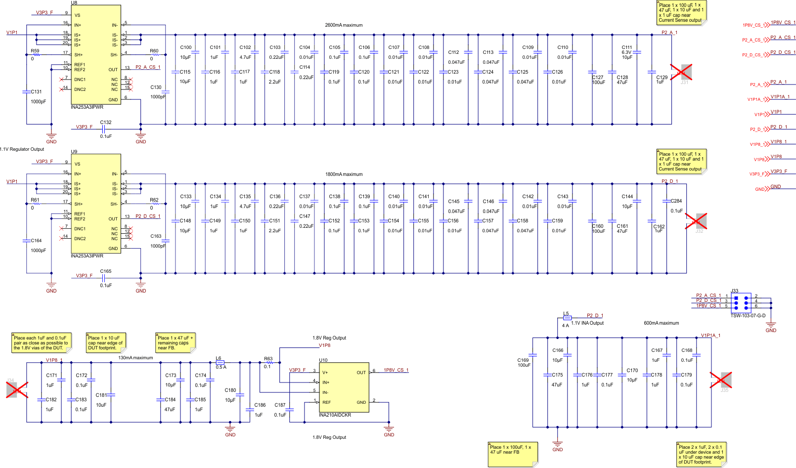 Figure 5-6 Schematic – Retimer 0 Current Sense
and Decoupling
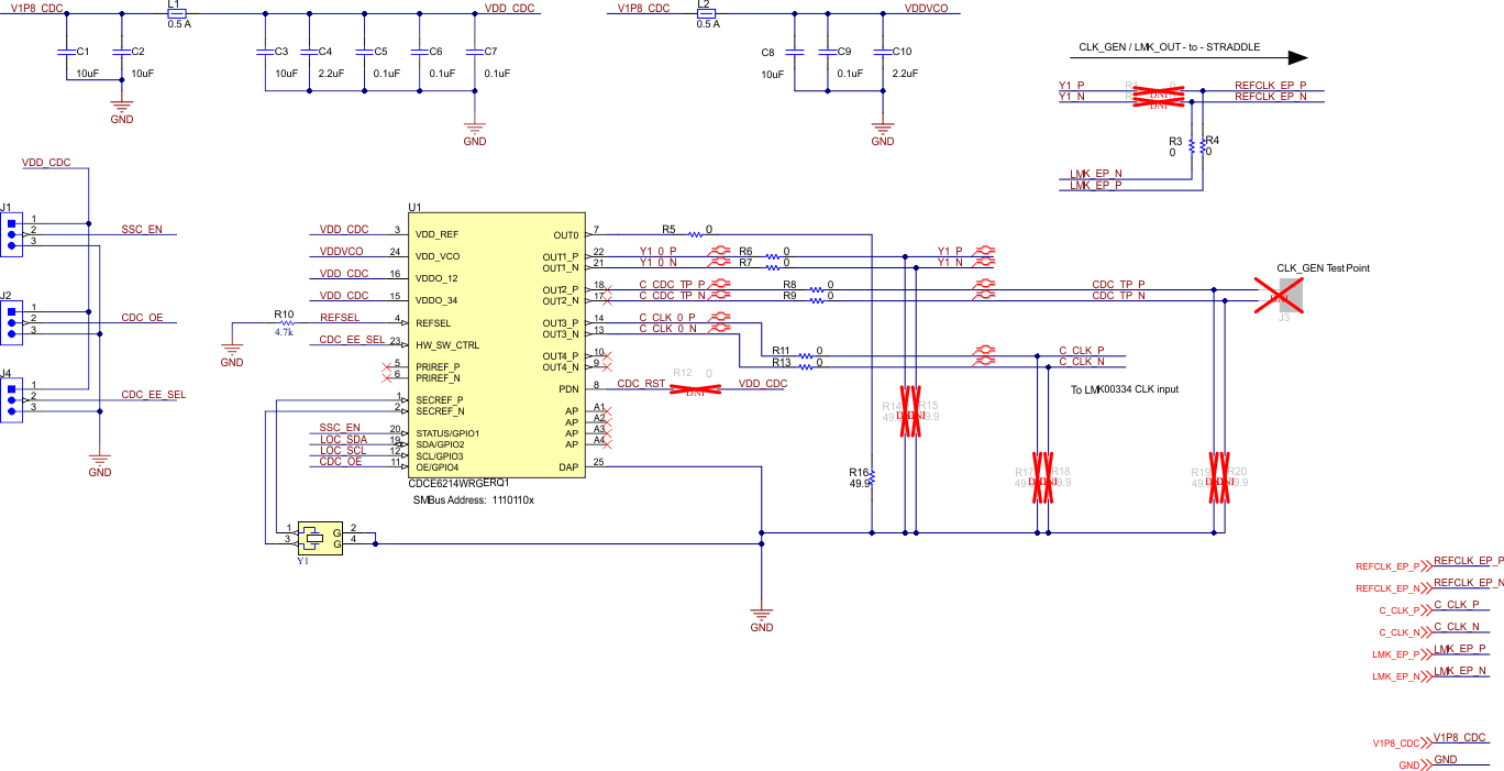 Figure 5-7 Schematic – PCIe Gen4 Clock
Generation
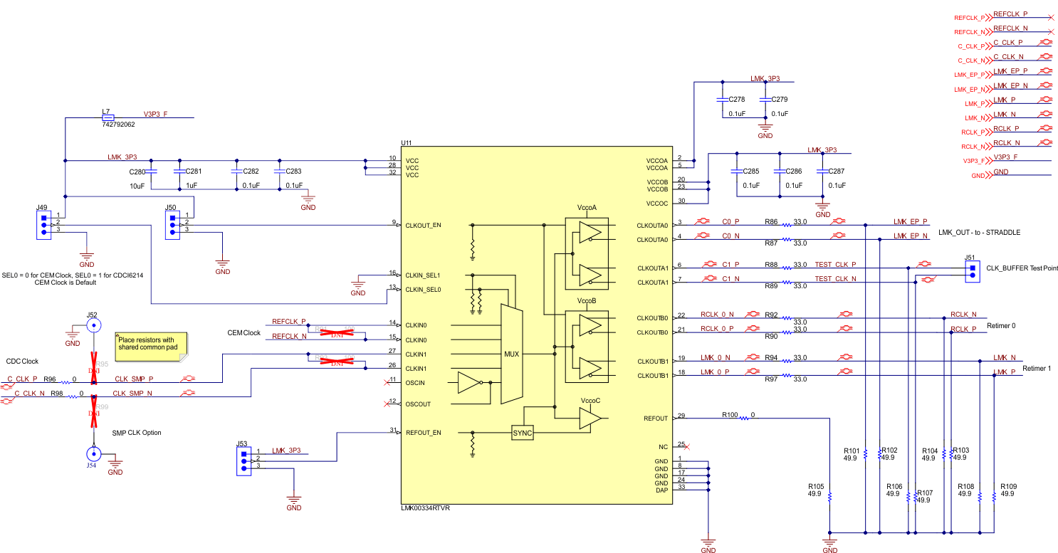 Figure 5-8 Schematic – PCIe Gen4 Clock
Buffer
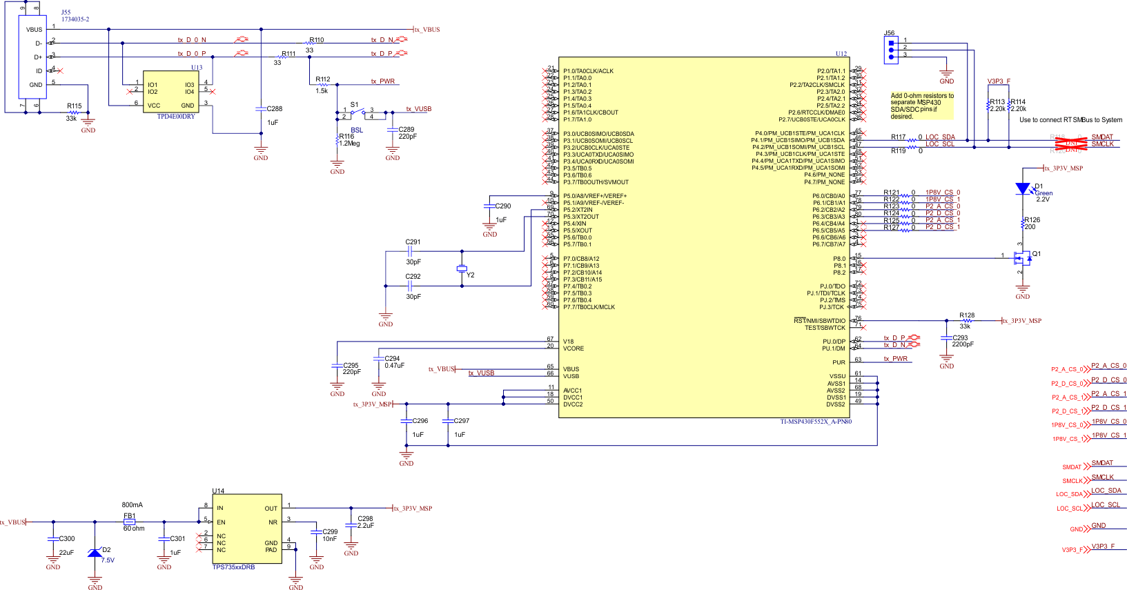 Figure 5-9 Schematic – MSP430
Microcontroller