SLVU276A February 2009 – October 2021 TPS54332
3.1 Layout
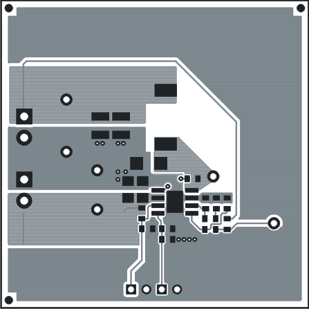
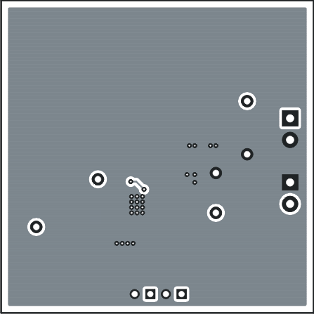
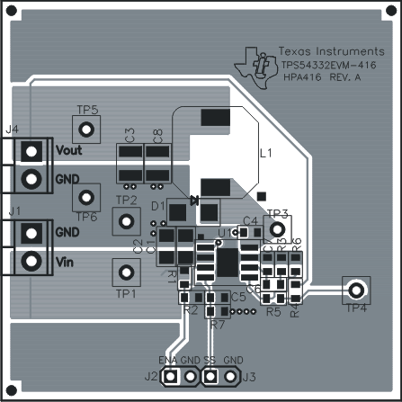
Figure 3-1 through Figure 3-3 shows the board layout for the TPS54332EVM-416. The top-side layer of the EVM is laid out in a manner typical of a user application. The top and bottom layers are 2-oz. copper.
The top layer contains the main power traces for VIN, VOUT, and VPHASE. Also on the top layer are connections for the remaining pins of the TPS54332 and a large area filled with ground. The bottom layer contains ground and a signal route for the BOOT capacitor. The top and bottom and internal ground traces are connected with multiple vias placed around the board including ten vias directly under the TPS54332 device to provide a thermal path from the top-side ground plane to the bottom-side ground plane.
The input decoupling capacitor (C2) and bootstrap capacitor (C4) are all located as close to the IC as possible. In addition, the voltage set-point resistor divider components are also kept close to the IC. The voltage divider network ties to the output voltage at the point of regulation, the copper VOUT trace past the output capacitors, C3 and C8. For the TPS54332, an additional input bulk capacitor can be required, depending on the EVM connection to the input supply.
 Figure 3-1 TPS54332EVM-416 Top-Side Layout
 Figure 3-2 TPS54332EVM-416 Bottom-Side Layout
 Figure 3-3 TPS54332EVM-416 Top-Side Assembly