-
Discrete Fault Detection Circuit for the TPS9261x-Q1 SLVAFE5 September 2022 TPS92610-Q1 , TPS92611-Q1 , TPS92612-Q1 , TPS92613-Q1
-
Discrete Fault Detection Circuit for the TPS9261x-Q1
Discrete Fault Detection Circuit for the TPS9261x-Q1
Abstract
Vehicle electronic fault detection is an important capability implemented in vehicles today to report what specific fault has occurred in an electronic system. This fault detection allows the vehicle to communicate the detected fault through LED indicators on the cluster, the onboard diagnostics port (OBD), and potentially over a wireless Wi-Fi®, 4GLTE, or 5G connection. Currently, the TPS9261x-Q1 family of devices features built in fault detection for open load (OL), short to ground (SG), short to battery (SB), and overtemperature (OT) faults that can occur on the LED driver output. However; there is only a single generic fault output to signal when any of the previously-listed faults have occurred in the system and therefore no way for the local MCU to distinguish what specific fault has taken place. This application note demonstrates a cost-effective method to implement a discrete fault detection circuit to report what specific fault has occurred on the TPS9261x-Q1 output to a local MCU.
Trademarks
Wi-Fi® is a registered trademark of Wi-Fi Alliance.
PSpice® is a registered trademark of Cadence Design Systems, Inc.
All trademarks are the property of their respective owners.
1 Introduction
Vehicle manufacturers greatly benefit from implementing circuits with detailed fault detection capabilities because this fault information can be shared with the driver through screen or LED indicators, with mechanics through the OBD port, and even to an OEM database or smart phone application over Wi-Fi, 4GLTE, or 5G wireless connections. The TPS9261x-Q1 family of LED drivers has the capability to detect an over temperature (OT), short to ground (SG), and open load (OL) or short to battery (SB) condition. However, there is only a single fault output to indicate if any of the above faults has occurred. This application note covers a method to detect these faults when implementing the TPS9261x-Q1 to drive off board LEDs.
2 TPS9261x-Q1 Fault Detection and Discrete Fault Detection Introduction
Before covering discrete fault detections, the device behavior during each fault condition must be understood.
Table 2-1 as published in the TPS92611-Q1 Automotive Single-Channel Linear LED Driver data sheet shows the expected behavior of the device during the four different fault conditions (OL,SB, SG, and OT).
| FAULT BUS STATUS | FAULT TYPE | DETECTION MECHANISM | CHANNEL STATE | DEGLITCH TIME | FAULT BUS | FAULT HANDLING ROUTINE | FAULT RECOVERY |
|---|---|---|---|---|---|---|---|
| FAULT floating or externally pulled up | Open-circuit or short-to-supply | V(IN) – V(OUT) < V(OPEN_th_rising) | On | t(OPEN_deg) | Constant-current pulldown | Device works normally with FAULT pin pulled low. Device sources I(retry) current when PWM is LOW. Device keeps output normal when PWM is HIGH. | Auto recover |
| Short-to-ground | V(OUT) < V(SG_th_rising) | On | t(SG_deg) | Constant-current pulldown | Device turns output off and retries with constant current I(retry), ignoring the PWM input. | Auto recover | |
| Over- temperature |
TJ > T(TSD) | On or off | t(TSD_deg) | Constant-current pulldown | Devices turns output off. | Auto recover | |
| Externally pulled low | Device turns output off | ||||||
When the device PWM pin input is high (output is on) during an open load or short to battery condition, the TPS9261x-Q1 detects an open load or short to battery has occurred and pull the fault pin low. The device continues to try and source the set current to the output every time PWM is set high. However, little to no current flows through the device due to the output voltage being equal to the input voltage (battery). In a short to battery condition, it is clear that the output voltage equals the battery but during an open load condition, the output also equals battery due to the constant current control of the TPS9261x-Q1. With a high impedance on the output, the TPS92611x tries to source the designed output current but because the output has infinite impedance, the output voltage is limited to the input voltage of the device. When PWM is set low and DIAG EN pin is high, the device sources a 1-mA I(retry) current to check if the open load or short to battery condition has been removed.
During a short to ground condition, when the PMW pin is high, the TPS9261x-Q1 detects a short to ground and pull the fault pin low. Before the fault is reported, the output voltage drops to approximately 0 V due to the TPS9261x-Q1 output sourcing the designed current into ground or close to 0 Ω. The output then is disabled once the fault is detected after t(SG_deg) and the device tries to source the 1-mA I(retry) current, regardless of the PWM pin, to detect if the short to GND has been removed.
Lastly, for an overtemperature condition, the device simply shuts off the output regardless of the state of the PWM pin. In this case, the output is disabled and there is no voltage on the output due to no current flowing from the device.
2.1 Discrete Fault Detection
Now that the expected behavior of the TPS9261x-Q1 is understood along with the condition of the OUT pin or output of the device, the discrete fault detection circuit must consider the fault behavior and expected output current or voltage during each fault condition. Figure 2-1 shows the discrete fault detection circuit block diagram.
2.2 Open Load vs Short-to-Battery Detection
The main approach for detecting between open load (OL) and short to battery (SB) is to measure the output voltage when the device output is disabled as shown in Figure 2-1. To do this, a voltage divider is required on the output of the TPS9261x-Q1 to verify that the comparator input is within a reasonable range and is not damaged. Remember, this pulls the output low in an open-load condition. Therefore, when a SB has occurred, the output voltage equals the battery, but in an OL condition, the output is pulled to ground. This now creates a detectable logical difference between the SB and OL conditions when the TPS9261x-Q1 output is disabled as shown in Figure 2-2.
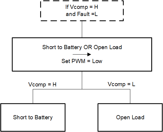 Figure 2-2 Short to Battery (SB) or Open Load (OL) Logic Flowchart
If the fault pin is initially triggered and the comparator output Vcomp is HIGH, then a SB or OL has occurred. Thus, to differentiate between the two faults, the PWM pin must be pulled LOW. Then, if Vcomp stays HIGH a short to battery has occurred and if Vcomp is LOW an open load fault has occurred. However, if DIAGEN is pulled high, the device sources the 1-mA I(retry) current preventing the output from ever being disabled in either OL or SB conditions. Nevertheless, the I(retry) current can be compensated for by the voltage divider on the output. The resistor values can be selected so that when the 1-mA current is sourced by the LED driver, the voltage on the output is lower than the battery voltage during an OL condition. Now the comparator can be configured to compare the output voltage and the voltage expected during OL conditions when I(retry) is sourced through the resistive divider. Additionally, the fault pin is now released during an OL condition after the PWM pin is pulled low and the I(retry) current is sourced due to the output voltage dropping below battery voltage and causing the Vin – Vout to be greater than V(OPEN_th_rising) (OL, SB fault condition from Table 2-1). Figure 2-3 and Figure 2-4 show the SB and OL conditions with the 1-mA I(retry) when PWM is LOW.
Another method to avoid I(retry) completely is to disable the OL and SB fault detection by pulling the DIAGEN pin LOW. However, the device no longer pulls fault LOW in an OL or SB condition. This can be valid due to the comparator detecting this fault but when the DIAGEN pin is set HIGH the fault pin adds an additional level of robustness to the fault detection scheme.
2.3 Short to Ground vs Overtemperature Detection
The next faults to detect are short-to-ground (SG) and overtemperature (OT) conditions. Figure 2-5 shows the SG condition.
In both SG and OT conditions, the output is disabled and the output voltage either drops to 0 V if either fault occurs when PWM is high, or stays at 0 V when transitioning the PWM pin from low to high during either fault condition. Therefore, the output voltage comparator does not help distinguish between the SG and OT faults. However, the devices built-in detection of SG and OT detects both faults and pulls the fault pin LOW. To distinguish between a SG and OT condition, the local MCU can simply adjust the PWM pin control of the TPS9261x-Q1 output. If the fault pin is pulled low by the LED driver but the comparator output has not triggered a SB or OL condition, the MCU can logically conclude that either a SG or OT condition has occurred. Next, the MCU can hold the PWM pin low for 300 ms to 500 ms to check if the LED driver has overheated. By pulling the PWM pin low, the MCU allows the TPS9261x-Q1 time to cool off and avoid any self-heating. If an OT condition has occurred, during the 200-ms to 500-ms wait time, the LED driver clears the fault after the 15°C hysteresis has been cleared (specified in the TPS9261x-Q1 data sheet). The MCU can then drive the PWM pin high at the dedicated PWM frequency and duty cycle to monitor if the fault pin is triggered again due to the LED driver overheating. Figure 2-6 shows the logic flowchart for distinguishing between SG and OT.
If the PWM pin is held HIGH and the comparator output (Vcomp) is LOW while the fault pin is LOW then a SG or OT has occurred. After the MCU holds the PWM pin low for 200 ms as shown in Figure 2-6, the fault pin state can be checked to determine if an OT event has occurred. If there is a SG, the fault pin stays low unless the short has been cleared. Therefore, some simple logic and control of the PWM pin can be implemented to detect if a SG or OT condition has occurred. Testing can be performed to understand what conditions cause the TPS9261x-Q1 to overheat.
2.4 Fault Detection Logic Summary
Figure 2-7 illustrates final flow of logic of the fault detection circuit.
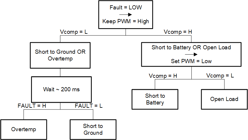 Figure 2-7 Discrete Fault Detection Logic
Flowchart
Figure 2-7 Discrete Fault Detection Logic
FlowchartAs Figure 2-7 shows, the comparator output (Vcomp), is used to distinguish if a SG, OT or SB, OL has occurred. If a SB or OL has occurred, Vcomp can be used to further distinguish between the two after PWM is pulled LOW. For SG, OT conditions, the fault pin is used along with the PWM pin to distinguish between a SG or OT fault.
3 Discrete Fault Detection Circuit Details
The discrete fault detection circuit utilizes the ATL431LI-Q1 device as a comparator to monitor the TPS9261x-Q1 output voltage. The ATL431LI-Q1 is a high bandwidth low IQ programmable shunt regulator that can act as a comparator in open loop mode. Additionally, the device has an internal reference voltage of 2.5 V and works well across temperature providing an accurate output voltage measurement. For more information on the ALT431LI-Q1 performance across temperature, see Using the TL431 for Undervoltage and Overvoltage Detection application note. The ATL431LI-Q1 output (Vcomp) is used to differentiate between OL, SB, and SG or OT conditions. Figure 3-1 illustrates the initial schematic with the fault detection circuit added on to the TPS9261x-Q1.
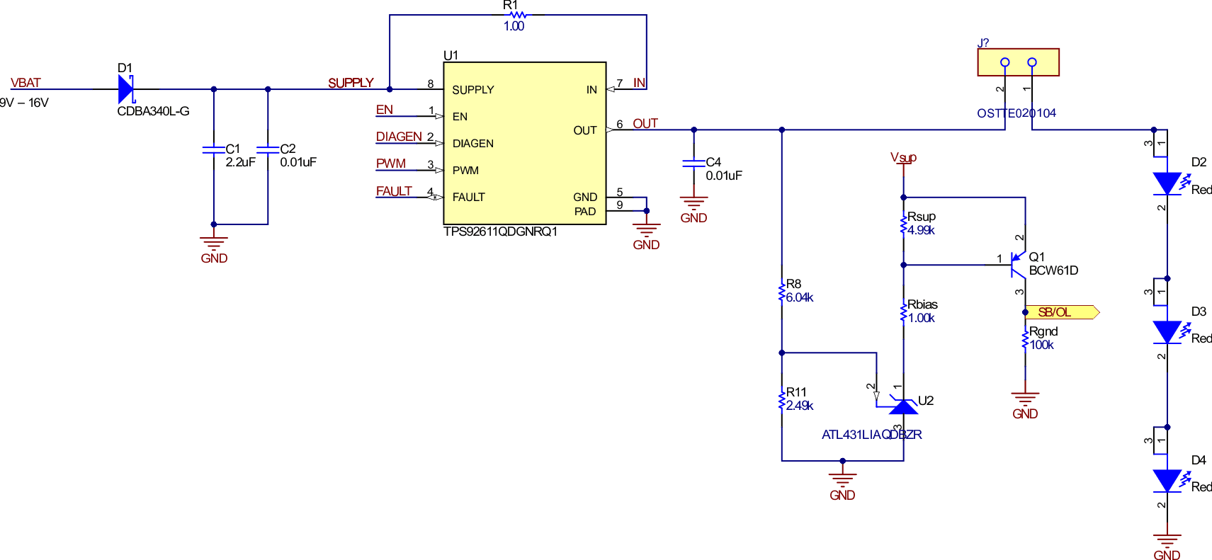 Figure 3-1 Discrete Fault Detection
Schematic
Figure 3-1 Discrete Fault Detection
SchematicA resistor divider must be used to properly divide the voltage going into the ATL431LI-Q1 from the output of the TPS9261x-Q1. This is to properly compare the OUT voltage to the reference voltage. In addition, this resistor ladder creates the trip point (where the comparator output changes). A trip point of 8.5 V was used for the tests in Section 3.1 to Section 3.4. To verify the resistor ladder behaves as expected, the total series resistance (Rtotal) of the resistive divider R8 and R11 must be approximately 8.5 kΩ. Due to the I(retry), a Rtotal that is too large causes the output and input voltages to be close to equal and therefore the ATL431LI-Q1 comparator does not trigger. Rsup and Rbias are used in accordance to Using the TL431 for Undervoltage and Overvoltage Detection application note to verify that the BJT has an appropriate voltage drop and that the ATL431LI-Q1 is not sinking excess current. Rgnd is utilized to pullup the SB, OL output to Vsup. Additionally, a BJT is used to verify that the ATL431LI-Q1 output swings from Vsup (3.3 V) to 0 V as described in the previously-referenced application note. Table 3-1 documents the logic truth table associated with the fault detection circuit. Each unique outcome is highlighted to show the logic for a microcontroller to differentiate between each fault scenario.
|
Condition |
PWM |
nFault |
Comparator Output (Vcomp) |
|---|---|---|---|
|
Normal Operation |
L |
H |
L |
|
H |
H |
L |
|
|
Short to GND, Over Temperature |
L |
L |
L |
|
H |
L |
L |
|
|
Short to Vbat |
L |
L |
H |
|
H |
L |
H |
|
|
Open Load |
L |
H |
L |
|
H |
L |
H |
3.1 Simulation
The fault detection circuit was created on PSpice® and an independent voltage source was used to simulate different voltage conditions on the TPS9261x-Q1 output. Figure 3-2 shows the circuit when the TPS9261x-Q1 output voltage is below the trip point of 8.5 V.
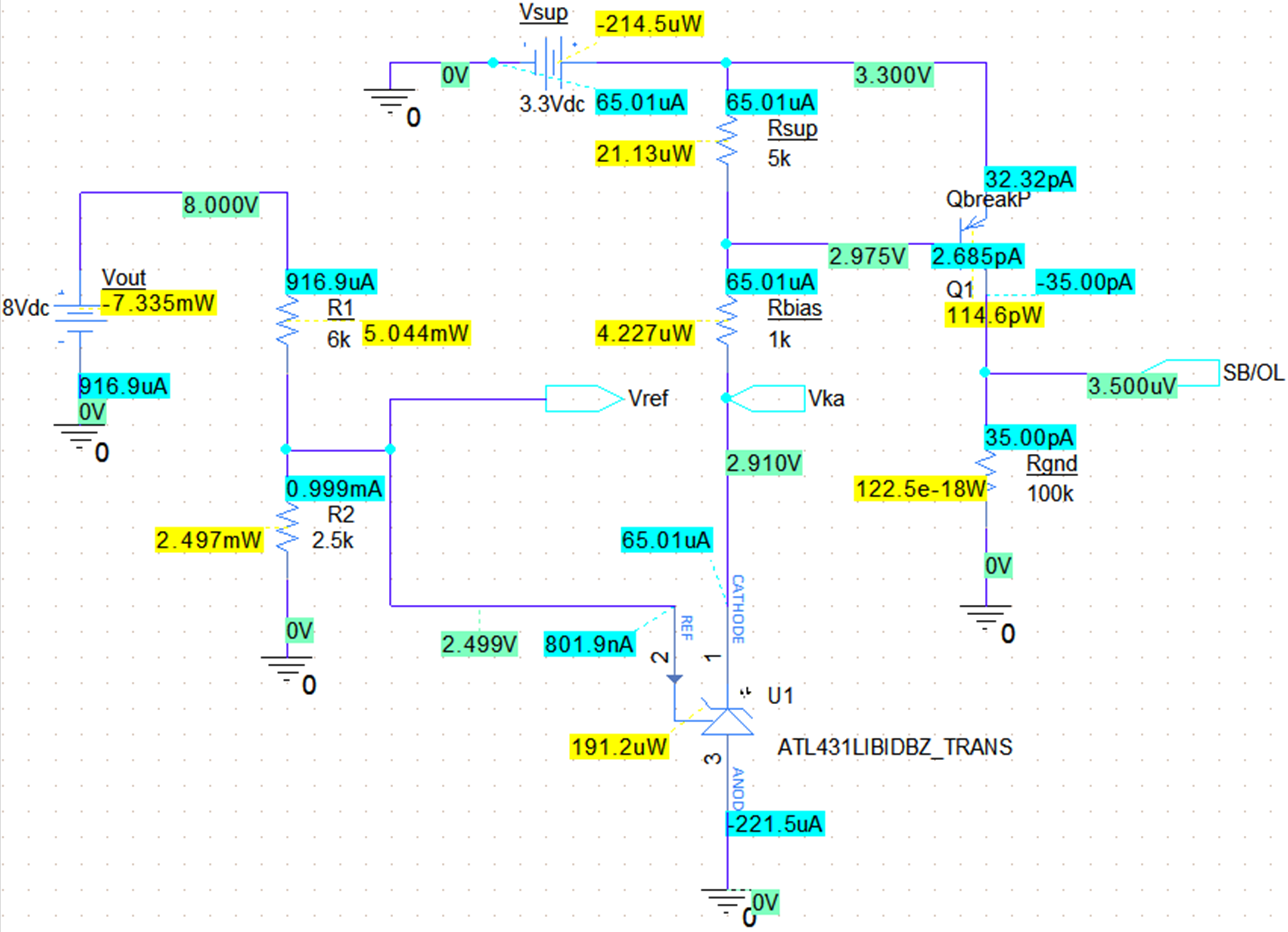 Figure 3-2 Simulation With TPS9261x-Q1
Vout Below the Trip Point
Figure 3-2 Simulation With TPS9261x-Q1
Vout Below the Trip PointAn 8-V voltage was applied to the fault detection circuit and with accordance to the truth table in Table 3-1. A proper LOW output is shown at SB/OL. Figure 3-3 shows the circuit when a voltage above the trip point of 8.5 V is present.
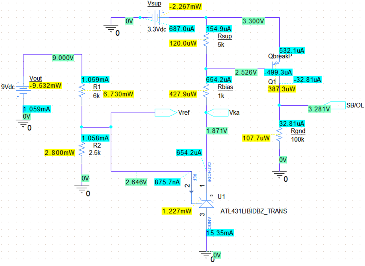 Figure 3-3 Simulation With TPS9261x-Q1
Vout Above the Trip Point
Figure 3-3 Simulation With TPS9261x-Q1
Vout Above the Trip PointA voltage of 9 V was applied to the fault detection circuit and with accordance to Table 3-1 the Vcomp output is HIGH as shown on SB/OL.
3.2 PCB Implementation
Figure 3-4 illustrates the PCB layout in a 2D view and Figure 3-5 utilizes a 3D view.
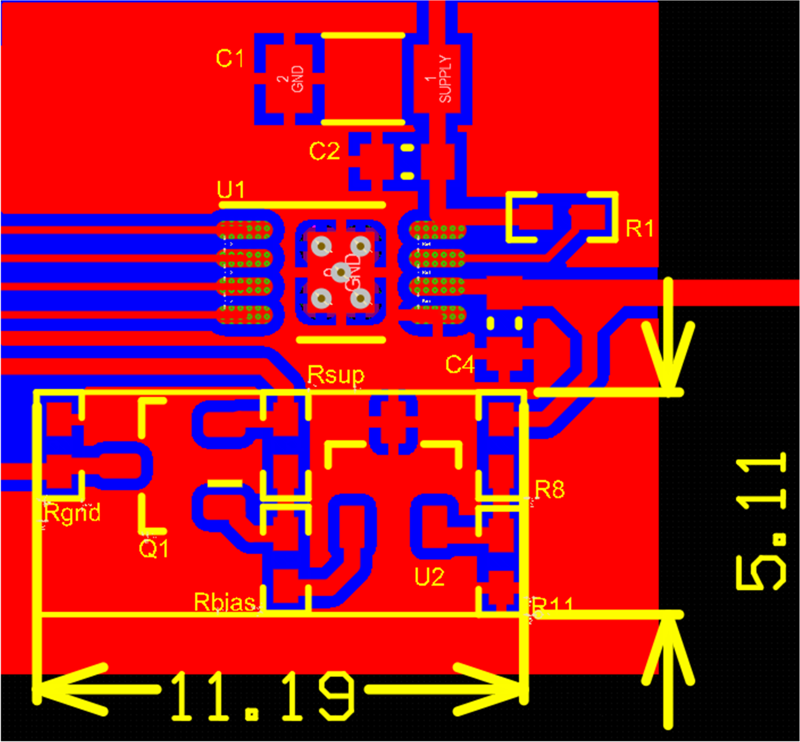 Figure 3-4 2D Fault Detection Circuit
Layout
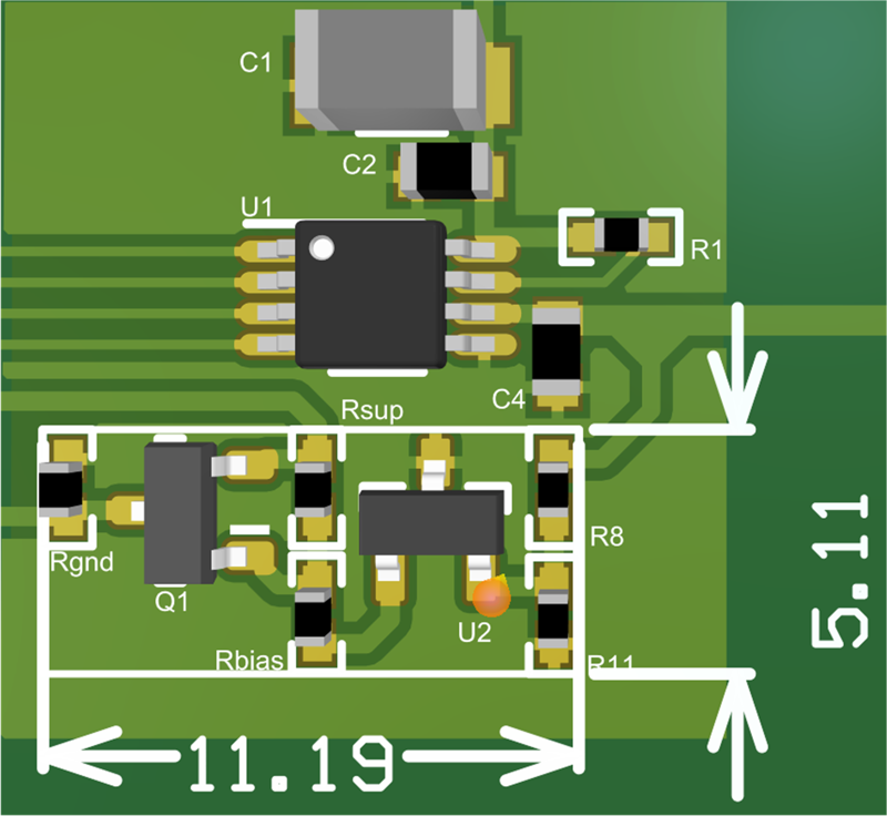 Figure 3-5 3D Fault Detection Circuit
Layout
Figure 3-5 3D Fault Detection Circuit
LayoutThe fault detection circuit was added in conjunction to the TPS92611-Q1 EVM and highlighted in silk screen on the layout. As shown in the layout, the footprint for the fault detection circuit is compact, only requiring an area of 11.19 mm × 5.11 mm (440.55 mil × 201.18 mil).