Stability Analysis and Design of D-CAP2 and D-CAP3 Converter – Part 2: How to Select Feedforward Capacitor
Trademarks
All trademarks are the property of their respective owners.
1 Introduction
D-CAP series control schemes are widely used in notebook, server, EP power and many other areas due to the advantages of good dynamic performance and less external components [1-2]. The zero formed by output capacitor ESR is used for loop compensation in the original D-CAP control [3- 4]. For some application with small ESR output capacitor, the zero generated by the internal ripple injection circuit can be used for compensation instead of the ESR zero in D-CAP2/D-CAP3 control. In the previous application report https://www.ti.com/lit/pdf/SLVAF11, it is introduced that a simplified method for D-CAP2/D-CAP3 converter stability design is to ensure the ripple injection zero inside bandwidth [5]. On the basis, the output capacitor selection limits are deducted for application design. However, the bandwidth will decrease with increasing output voltage in D-CAP control loop and the ripple injection zero is hard to be kept inside bandwidth. In this condition, the feedforward capacitor, that can provide an additional pair of zero and pole in the loop, can be used to ensure system stability. The detailed analysis and selection method of feedforward capacitor Cff are introduced in this application report.
2 Why We Need Cff in High Output Voltage D-CAP2/3 Converter for Stability
The bode plots of D-CAP2/D-CAP3 converters are shown as Figure 2-1. After the LC double poles frequency ω0 related with inductance and output capacitance, the slope of loop gain can be approximately seen as changing from 0 to -40dB/decade. With the zero injected by the internal ripple injection circuit, the slope becomes – 20dB/decade at 0dB, which could bring sufficient phase margin [7].
 D-CAP2 (b) D-CAP3 Converter") Figure 2-1 Bode Plot
of (a) D-CAP2 (b) D-CAP3 Converter
Figure 2-1 Bode Plot
of (a) D-CAP2 (b) D-CAP3 ConverterFor a stable D-CAP2/3 converter, if output voltage is increased with no other changes, the system will tend to become unstable, as shown in Figure 2-2. Since the gain before double poles frequency equals to Acp*Vref/Vo, system gain and crossover frequency ωcross will decrease with increasing Vo. If ωcross becomes lower than the frequency of ripple injection zero ωRI, system will have a -40dB/decade slope at 0dB, which may cause insufficient phase margin.
 low Vo with
-20dB/Decade Crossing (b) high Vo with
-40dB/Decade Crossing") Figure 2-2 Loop Gain
of a D-CAP2 Converter (a) low Vo with
-20dB/Decade Crossing (b) high Vo with
-40dB/Decade Crossing
Figure 2-2 Loop Gain
of a D-CAP2 Converter (a) low Vo with
-20dB/Decade Crossing (b) high Vo with
-40dB/Decade CrossingFor some D-CAP2/3 converters similar to TPS548D22, the ripple injection zero frequency ωRI is adjustable with external configuration (sometimes named as ramp time constant, the ramp here is the ripple injection, time constant is the reciprocal of angular frequency). For TPS548D22, the Vref can also be adjusted for different output voltage to change ωcross. Those features can both help to adjust the relation of ωcross and ωRI and achieve -20dB/decade crossing.
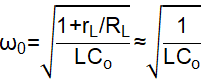
But for most D-CAP2/3 devices to achieve easy design, the ripple injection zero frequency and reference voltage are fixed. So the LC double poles frequency ω0 must be increased for bandwidth improvement to ensure -20dB/decade slope at 0dB, as shown in Figure 2-3. However, it can be seen from Equation 1 that the inductance and output capacitance must be reduced to increase LC double poles frequency, which will cause large output ripple and noise. That causes the contradiction between output ripple and stability for D-CAP2/3 converters.
 High Vo with
-40dB/Decade Crossing (b) Reducing L or
Co for -20dB/Decade Crossing") Figure 2-3 Loop Gain
of a D-CAP2 Converter (a) High Vo with
-40dB/Decade Crossing (b) Reducing L or
Co for -20dB/Decade Crossing
Figure 2-3 Loop Gain
of a D-CAP2 Converter (a) High Vo with
-40dB/Decade Crossing (b) Reducing L or
Co for -20dB/Decade CrossingIn application report https://www.ti.com/lit/pdf/SLVAF11, TPS568230 was used as an example to illustrate the stability design method for a 1.5 V Vo low output voltage application. Here the case with 5 V Vo is shown to reflect the contradiction between output ripple and stability in high output voltage application.
The condition for analysis is: Vin=12 V, Vo=5 V, Ioutmax=8 A, fsw=600kHz. First, the range of inductance can be got as 1.52uH-3.04uH, according to the principle to limit inductor current ripple as 20%-40% of Ioutmax.
Select inductor 744311220 L=2.2uH. Based on the previous proposed selection method of output capacitor, we could get the limits of Co as 4.7uF-22.3uF. With the upper limit Co=22.3uF, the output voltage ripple is too large to meet the requirement for lots of application.
It is obvious that reducing L or Co is just a trade-off solution between output voltage ripple and stability. Compared to that, adding feedforward capacitor Cff is a better solution to ensure converter stability.
3 Effects of Feedforward Capacitor on the Loop
 Figure 3-1 Scheme of Feedback Divider
Including Feedforward Capacitor
Figure 3-1 Scheme of Feedback Divider
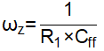
Including Feedforward CapacitorThe effects of adding feedforward capacitor in the feedback divider are studied in the application report [6]. A feedback divider including Cff is shown as Figure 3-1. Cff will introduce a pair of zero and pole in the converter loop. The angular frequency of the introduced zero and pole are:

The effects of the zero and pole introduced by Cff are shown as Figure 3-2.
Cff has both effects on the loop gain and phase. The loop gain is increased to boost bandwidth and optimize transient response. Also, the phase is boosted to increase the phase margin for system stability.
In application notes [2,8], some methods have been proposed to use Cff for phase margin enhancement. But in those methods, the bode plot results without Cff are always needed to get recommended Cff value. That feature makes those Cff selecting methods more applicable in the solution validation process but not in the application design process.
A new method to choose Cff is proposed in this application report. The bode plot results without Cff are not needed to get the recommended Cff value in this method, which makes it more applicable in application design.
4 Cff Choose Method
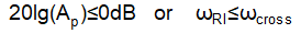
This method is implemented by letting the gain cross 0dB with -20dB/decade slope [7]. To be noted, -20dB/decade gain at 0dB is not a necessary condition for stability. So this method just provides an allowable range for Cff and it doesn’t mean the converter will be unstable if Cff exceeds this range.
For the case as Figure 4-1(a) when the ripple injection zero frequency ωRI is larger than bandwidth, we can add the Cff zero ωz inside bandwidth, then the loop gain can cross 0dB with -20dB/decade, as shown in Figure 4-1(b).
In the case as Figure 4-2, the zero and pole introduced by Cff are both added inside bandwidth and the system stability can still be ensured. Although the slope of loop gain becomes -40dB/decade again after the pole ωp, the loop gain increasement with Cff makes the bandwidth increased and the ωRI becomes smaller than bandwidth. A -20dB/decade crossing is achieved and system will have enough phase margin.
In the case as Figure 4-3, both the zero and pole introduced by Cff are inside bandwidth, but the ripple injection zero frequency ωRI is still larger than the bandwidth. At this condition, the loop gain will still cross 0dB with -40dB/decade, which can’t ensure the system phase margin.
Above all, we can conclude two restrictions to achieve a stable state with -20dB/decade crossing after adding feedforward capacitor:
A. ωz<ωcross; B. avoiding the condition as Figure 4-3.
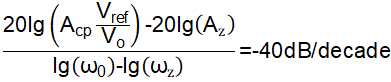
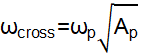
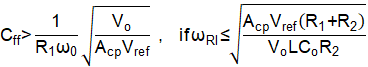
First we could deduct the limit for restriction A. Based on Figure 4-4, we can know that ωz<ωcross can be achieved by ensuring ωz<ωc. The expression of ωc is as equation (4). With equations (2) and (4), the lower limit of Cff is derived as equation (5).
 Figure 4-4 D-CAP2 Converter Loop Gain When
Adding ωz< ωcross
Figure 4-4 D-CAP2 Converter Loop Gain When
Adding ωz< ωcross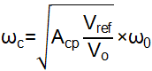
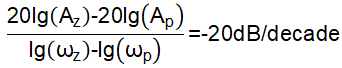
To get the limits for restriction B, we could know that Equation 6 corresponds the condition as Figure 4-3. Then the restriction B to avoid that condition corresponds to Equation 7.

where Ap is the amplitude of gain at ωp.
To get the expressions of Ap and ωcross, we can first get the relation between gain and frequency as Equation 8 through Equation 10.
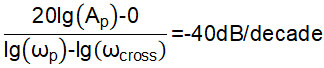
Substituting Equation 2 through Equation 3 into Equation 8 through Equation 10, the expressions of Ap and ωcross can be received as Equation 11 and Equation 12.
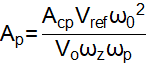
Substituting Equation 11 and Equation 12 into Equation 7, we can get Equation 13 as equation for restriction B.
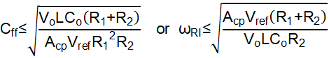
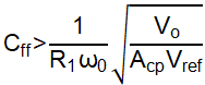
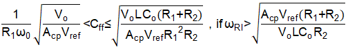
Combine the Equation 5 for restriction A and Equation 13 for restriction B, Equation 14 and Equation 15 are the limits for Cff.
At the meantime, the bandwidth after adding Cff should also be limited under 1/3*fsw. Since it is hard to give a unified method for the estimation of bandwidth and phase margin after adding Cff, it is suggested to verify with the help of simulation model or bench loop test results.
5 Application Design Example of D-CAP2/D-CAP3 Converter with Cff
Figure 5-1 is the design flow chart for D-CAP2/D-CAP3 converter with Cff. All the inductance and capacitance used in choosing Cff are effective value considering degrading.
Here TPS568230 is used as an example to illustrate the design method for a 5V Vo application. The condition of example is Vin=12 V, Vo=5 V, Ioutmax=8 A, fsw=600kHz.
First select voltage divider resistors R1(Rtop)=220 kΩ and R2(Rbottom)=30 kΩ to achieve 5 V output with 0.6 V reference voltage. Then, same as the analysis mentioned in section 2, the range of inductance can be got as 1.52 uH-3.04 uH, according to the principle to limit inductor current ripple as 20%-40% of Ioutmax. And we can select 744311220 inductor and its effective inductance with 8 A current is about 1.8 uH.
About 180uF output capacitance are used to meet output ripple requirement. Here the 885012108012 MLCC are used. With about 52.5% degrading at 5 V bias for the 47 uF capacitance, the effective capacitance of each MLCC is about 22.35 uF. Capacitance of 8 parallel MLCCs are 178.8 uF.
Then the method is used to select Cff. As Acp=29.3 and ωRI=270 k for TPS568230, we can get Cff>44 pF according to Equation 14 and Equation 15. Here we can choose 120 pF Cff.
6 Experimental Verification
The bode plot test result with 180 uF output capacitors and no Cff is shown in Figure 6-1 for comparison. It could be seen that the phase margin is 17.228 degree. The crossover frequency is about 18.54 kHz.
 Figure 6-1 Experimental Result without
Cff
Figure 6-1 Experimental Result without
CffFigure 6-2 shows the validation result with chosen Cff=120 pF using the proposed method. It can be seen that bandwidth is increased from 18.54 kHz to 47.22 kHz, while the phase margin is increased from 17.228 degree to 75.353 degree. Both dynamic performance and stability can be enhanced with the 120 pF Cff. That proves the effectiveness of the proposed method.
 Figure 6-2 Experimental Verification of
Proposed Method
Figure 6-2 Experimental Verification of
Proposed Method7 Conclusion
A selection method of feedforward capacitor is proposed in this application report for D-CAP2/D-CAP3 converters based on loop stability analysis. First, the necessity of adding Cff in some application with high output voltage is analyzed. Then the impacts of the Cff on the converter loop is introduced and a method to choose Cff for stability is proposed by ensuring -20dB/decade gain slope at gain crossover frequency. Compared with previous methods, the bode plot test results without Cff aren’t needed to get recommended Cff value, which makes the method more applicable in application design process. Finally, a detailed flow chart is given to help designing application of D-CAP2/D-CAP3 converter. The proposed method is verified by experiments.
8 References
- Frequency Domain Analysis of Fixed On-Time with Bottom Detection Control for Buck Converter, M. Lin, T. Zaitsu, T. Sato, and T. Nabeshima, IEEE IECON2010, pp.475-479
- Texas Instruments, D-CAP2TM Frequency Response Model based on frequency domain analysis of Fixed On-Time with Bottom Detection having Ripple Injection, application report.
- Texas Instruments, Loop Stability Analysis of Voltage Mode Buck Regulator with Different Output Capacitor Types – Continuous and Discontinuous Modes, application report.
- Understanding and Applying Current-Mode Control Theory, application report.
- Texas Instruments, Stability Analysis and Design of D-CAP2 and D-CAP3 Converter - Part 1: How to Select Output Capacitor, application report.
- Texas Instruments, Optimizing Transient Response of Internally Compensated dc-dc Converters With Feedforward Capacitor, application report.
- Feedback Control of Dynamic Systems, Gene F. Franklin, J. David Powell, Abbas Emami-Naeini.
- Texas Instruments, Designing a Feedforward Capacitor for LMR140x0, application report.
9 Appendix A
For TPS568230 Ioutmax=8 A, Vref=0.6 V. Co in the table are effective value considering degrading. The large Cff as 1000 pF can be allowed from loop stability view, but it could inject more high frequency noise into feedback and also might affect converter operation. The Cff theoretical calculation methods must be used combined with real situation and bench test results.
| Vin (V) | Vo (V) | fsw (kHz) | Rtop/Rbottom | Llimits (uH) | Lchoose(uH) | Co (uF) | Cff limit | Cff choose (pF) | PMtest (deg) |
|---|---|---|---|---|---|---|---|---|---|
| 6 | 2.5 | 600 | 95 kΩ/30 kΩ | 0.76-1.52 | 1 | 200 | Cff>56pF | 70 | 81.4 |
| 1000 | 50.8 | ||||||||
| 6 | 3.3 | 600 | 90 kΩ/20 kΩ | 0.77-1.55 | 1 | 200 | Cff>68 pF | 80 | 80.2 |
| 1000 | 47 | ||||||||
| 18 | 2.5 | 600 | 95 kΩ/30 kΩ | 1.12-2.24 | 1.5 | 200 | Cff>69 pF | 82 | 80 |
| 1000 | 63 | ||||||||
| 18 | 3.3 | 600 | 90 kΩ/20 kΩ | 1.4-2.81 | 2.2 | 200 | 100-236 pF | 110 | 83 |
| 220 | 75 | ||||||||
| 18 | 5 | 600 | 220 kΩ/30 kΩ | 1.88-3.76 | 2.2 | 200 | 51-147 pF | 62 | 72 |
| 140 | 77 |
IMPORTANT NOTICE AND DISCLAIMER
| TI PROVIDES TECHNICAL AND RELIABILITY DATA (INCLUDING DATASHEETS), DESIGN RESOURCES (INCLUDING REFERENCE DESIGNS), APPLICATION OR OTHER DESIGN ADVICE, WEB TOOLS, SAFETY INFORMATION, AND OTHER RESOURCES “AS IS” AND WITH ALL FAULTS, AND DISCLAIMS ALL WARRANTIES, EXPRESS AND IMPLIED, INCLUDING WITHOUT LIMITATION ANY IMPLIED WARRANTIES OF MERCHANTABILITY, FITNESS FOR A PARTICULAR PURPOSE OR NON-INFRINGEMENT OF THIRD PARTY INTELLECTUAL PROPERTY RIGHTS. |
| These resources are intended for skilled developers designing with TI products. You are solely responsible for (1) selecting the appropriate TI products for your application, (2) designing, validating and testing your application, and (3) ensuring your application meets applicable standards, and any other safety, security, or other requirements. These resources are subject to change without notice. TI grants you permission to use these resources only for development of an application that uses the TI products described in the resource. Other reproduction and display of these resources is prohibited. No license is granted to any other TI intellectual property right or to any third party intellectual property right. TI disclaims responsibility for, and you will fully indemnify TI and its representatives against, any claims, damages, costs, losses, and liabilities arising out of your use of these resources. |
| TI’s products are provided subject to TI’s Terms of Sale (www.ti.com/legal/termsofsale.html) or other applicable terms available either on ti.com or provided in conjunction with such TI products. TI’s provision of these resources does not expand or otherwise alter TI’s applicable warranties or warranty disclaimers for TI products. |
| Mailing Address: Texas Instruments, Post Office Box 655303, Dallas, Texas 75265
Copyright © 2020, Texas Instruments Incorporated |
