-
Parallel Operation of TPS2663 eFuses
Parallel Operation of TPS2663 eFuses
Trademarks
All trademarks are the property of their respective owners.
1 Introduction
The TPS2663 device incorporates protection features such as inrush current management, adjustable overcurrent limit, short-circuit protection, overvoltage and input reverse polarity protection. Figure 1-1 shows an application schematic of the TPS26631 feeding a downstream DC-DC converter in a PLC system. The capacitor CdVdT on the dVdT pin sets the output voltage slew-rate and hence the inrush current level where as the resistor RILIM sets the current limit (ILIM) which the device needs to limit to under fault conditions. The device offers a B-FET driver to control an external N-channel FET ‘Q1’ for reverse current and reverse polarity protection which simplifies designs requiring class-A performance during system tests like IEC61000-4-5 surge tests as well as input supply brown-out tests.
The maximum current the TPS2663 can support is up to 6 A. However the device can be used in parallel configuration with multiple TPS2663 devices to achieve higher output currents which is often required in many industrial systems. This report presents how the TPS2663 can be used in parallel operation to achieve higher output currents as well as to demonstrate the performance benefits it brings to the system with its integrated protection functions.
2 Parallel Configuration
The basic principle of eFuse parallel operation and the design considerations are covered in the Achieve 20-A Circuit Protection and Space Efficiency Using Paralleled eFuses Application Report(1). The same concept is applicable for TPS26631 parallel operation. The key points from the Achieve 20-A Circuit Protection and Space Efficiency Using Paralleled eFuses Application Report(1) are summarized in the rest of this section in the context of TPS26631.
- During start-up, equal current
sharing among the parallel-connected eFuses is needed to ensure successful
start-up. To achieve that,
- The UVLO, OVP, SHDNb pins of all the parallel-connected eFuses are connected together for synchronizing the ON or OFF operation
- The dVdT pins of all the eFuses are connected together to ensure uniform output ramp rate and equal dynamic power stress
- During steady-state operation, the current sharing is decided by the RDS(on) mismatch. The device having the lower RDS(on) shares more current than the rest of the devices. However, the self-heating effect due to positive temperature characteristics of the MOSFET helps to a larger extent towards equal load current distribution in parallel configuration.
- During overload operation, the inherent current source characteristic of eFuse forces all the parallel-connected eFuses to operate in current-limiting mode. For the TPS26631, each device should have its own current-limiting resistor (RILIM) as demanded by the internal current loop architecture.
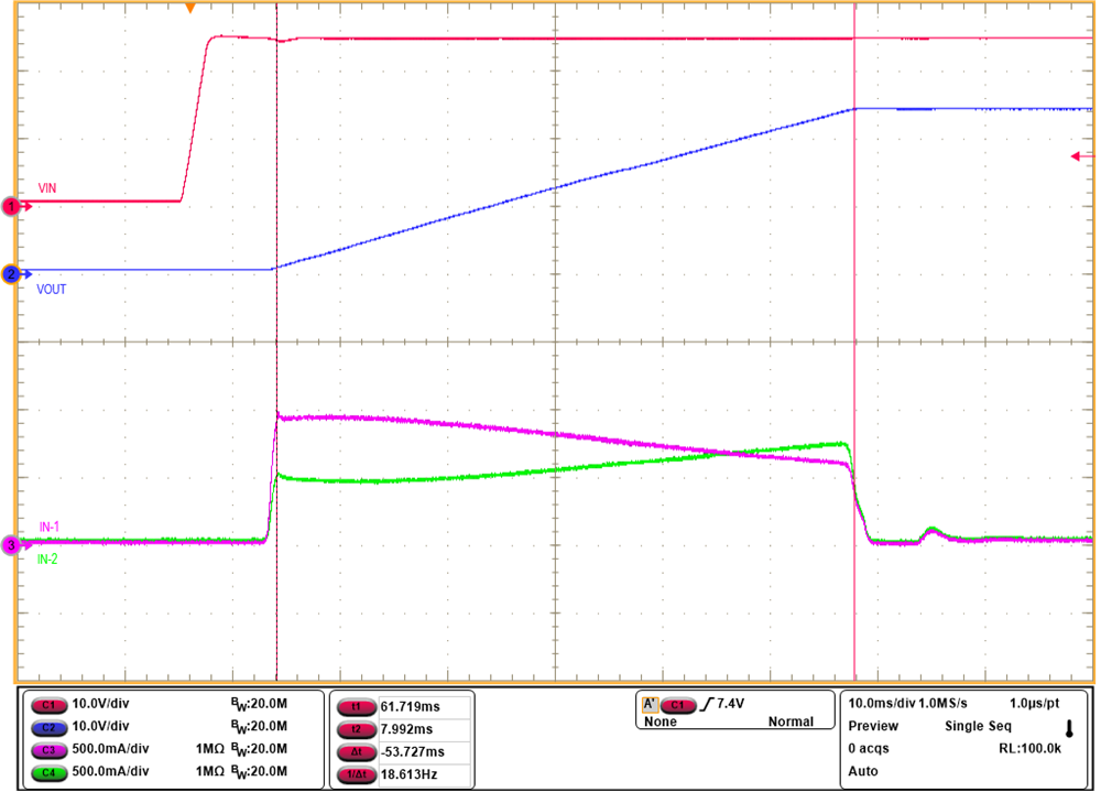 Figure 2-2 Current Sharing Between the Devices During Start-up in dVdT mode
Figure 2-1 illustrates the circuit configuration of two TPS26631 devices in parallel. A single blocking FET Q1 on the primary eFuse is enough for reverse current blocking. Figure 2-2 shows the current sharing during start-up with dVdT pins together. Even though the ramp rate of the dVdT pin is the same for both the devices, the mismatch in the internal dVdT gain and the internal FET characteristics leads to unequal current sharing during start-up. For uniform current distribution while starting up into large loads, current limited start-up is recommended as follows
- Leave dVdT pins OPEN
- Use RILIM resistor switch network at the ILIM pin. The RILIM_Low sets the inrush current. After successful start-up, PGOOD asserts high which sets the overload current limit as per (RILIM_Low || RILIM_High) at the ILIM pin
The modified parallel circuit configuration is illustrated in Figure 2-3 and the corresponding start-up waveform demonstrating equal start-up current between two TPS26631 devices is shown in Figure 2-4. In this application report, RILIM resistor switch network is considered in the design example as it ensures uniform current sharing under all the stressful events.
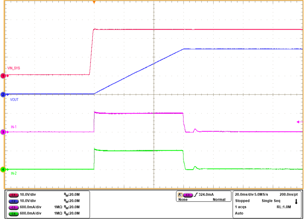 Figure 2-4 Current Sharing Between the Devices During Start-up in Current-Limit
Mode
Figure 2-4 Current Sharing Between the Devices During Start-up in Current-Limit
Mode3 Design Example
An example of designing four TPS26631 eFuse parallel circuits is considered in this section.
3.1 Design Requirements
Table 3-1 shows the design parameters for this application example.
| Design Parameter | Example Value |
|---|---|
| Typical input voltage, VIN | 24 V |
| Undervoltage lockout set point, VUV | 18 V |
| Overvoltage cutoff set point, VOV | 33 V |
| Inrush current limit, IINRUSH | 2.4 A |
| Maximum load current, IOUT | 22 A |
| IEC61000-4-5 Surge test level | ±500 V with 2-Ω generator impedance |
| Surge performance | Class-A |
3.2 Detailed Design Procedure
- Device selection
In this example, the TPS26631 variant is considered to highlight the current sharing during the 2 × pulse current support. For more information, see the Device Comparison Table in the TPS2663x 60-V, 6-A Power Limiting, Surge Protection Industrial eFuse data sheet for device selection. In a system where reverse current blocking is not required, the TPS1663 devices are recommended.
- ILIM setting
To limit the inrush current to 2.4 A (that is, 0.6 A per device), the RLIM_Low is selected as 30 kΩ. Considering the cumulative current limit accuracy of 10% and to support maximum load current of 22 A, the current limit is set at 24 A (that is, 6 A per device). This results in 3.33-kΩ value for RLIM_High.
- Undervoltage Lockout and
Overvoltage Set Point
The resistors R1, R2, and R3 are selected as 887 kΩ, 29.4 kΩ, and 34 kΩ, respectively, to set 18 V as undervoltage lockout and 33 V as overvoltage trip point.
- dVdT capacitor
Leave dVdT pins OPEN because the RILIM resistor switch network is considered in this design.
- IMON resistor
In parallel configuration, IMON pins of all the devices can be combined to monitor the total system current. The maximum value of the RIMON resistor can be determined by Equation 1. The maximum VIMON voltage is determined by the ADC input range and it is 3.3 V.
Equation 1.Where GAINIMON is 27.9 µA/A (typ) and IOUT_max is 48 A because of 2 × overcurrent pulse support with the TPS26631.
Using Equation 1, we get RIMON as 2.46 kΩ.
- PGOOD, FLTb
The output of these pins are used only from the primary eFuse to control downstream load and these pins are left OPEN for the rest of the parallel TPS26631 devices.
- PGTH
The TPS2663 device uses PGTH as the output load voltage monitor and to set the downstream loads UVLO threshold. The voltage at PGTH determines the way the TPS2663 recovers during the system faults. During the fault recovery instance, if the V(PGTH) level is above V(PGTHF), then the internal FET turns ON with a fast slew rate to meet Class-A system performance during surge events with optimal output buffer capacitance.
Typically, the minimum operating voltage of the DC-DC converter designed for 24-V rail is at 15 V. Assuming UVLO to be at 20% lower level, VUVLO_DC-DC = 12 V. Use Equation 2 to calculate R4 and R5.
Equation 2.V(PGTHF) = 1.14 V. Assuming R5 = 56 kΩ, R4 comes out to be approximately 499 kΩ.
- Output Buffer Capacitor,
COUT
During the surge event TSURGE, the output capacitor COUT of the TPS2663 provides energy to the load. The COUT should be selected such that the output voltage does not drop below VUVLO_DC-DC during TSURGE interval. Use Equation 3 to compute the required buffer capacitor COUT:
Equation 3.where
- P(DC-DC) = max load power ≈ 500 W
- TSURGE ≈ 1 ms
- V(IN_SYS) = 24 V
- V(UV_DC-DC) = 15 V
The value is determined to be COUT = 2.85 mF. Choose a capacitor with ±10% tolerance, COUT = 3 mF / 35 V electrolytic capacitor.
- Input and output
capacitors
A minimum of 0.1-µF ceramic decoupling capacitor is recommended at the input and the output for each of the eFuse.
- Reverse current blocking
FET
Choose at least a 80-V rated N-channel FET. Two CSD19532Q5B FETs are used in parallel to support continuous load current of 22 A.
- TVS diode and Schottky
diode
For clamping ±500-V, 2-Ω surge voltages with in the absolute maximum voltage rating of the TPS2663 device, bidirectional TVS diode SMCJ36CA is used at the input. Similarly, to clamp the negative voltages at the output during fast turn-off events, a Schottky diode B560C-13-F is recommended at the output.
3.3 Performance Results
Figure 3-1 shows the PCB with four TPS26631 devices.
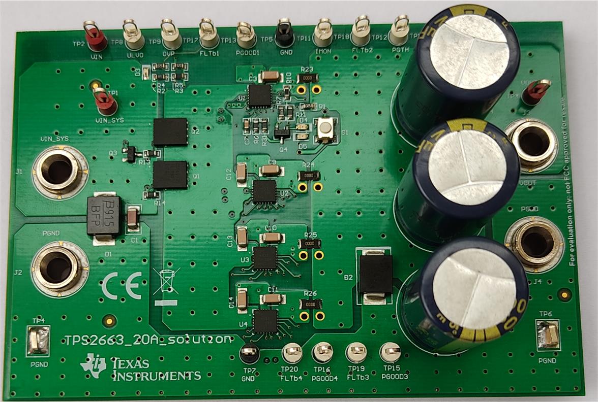 Figure 3-1 Evaluation Board With Four
TPS26631 Devices in Parallel
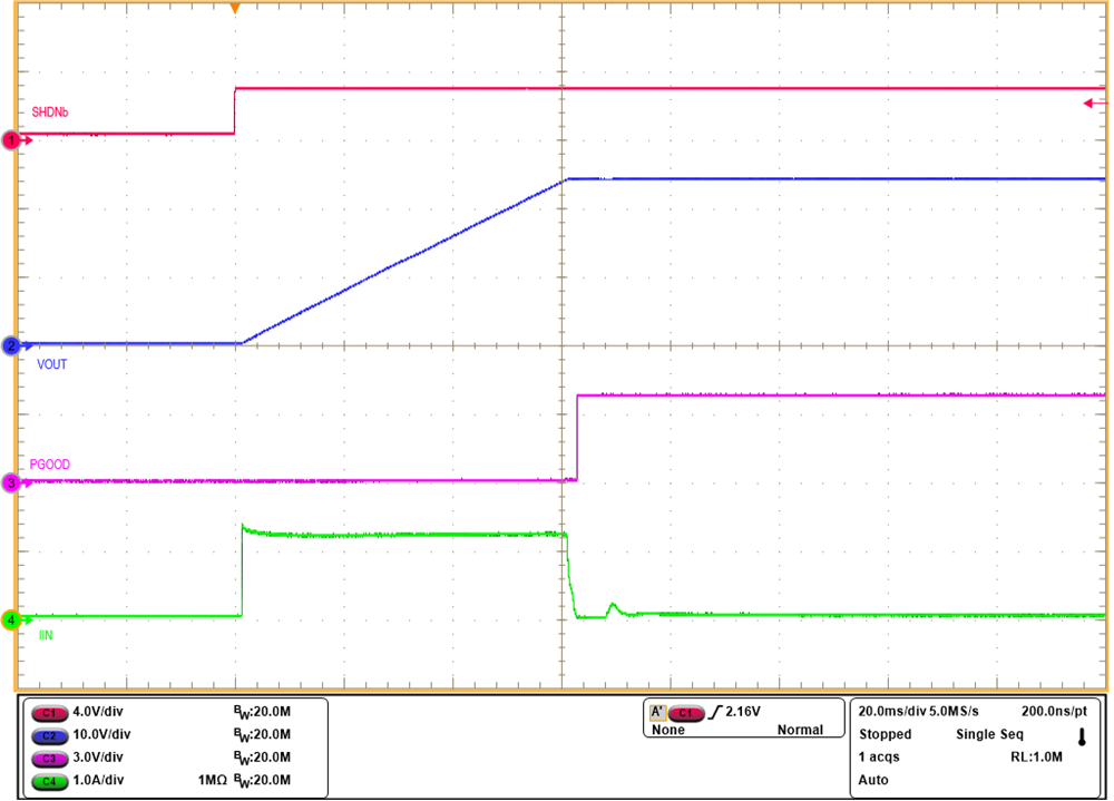 Figure 3-2 Turn-on Control With
SHDN
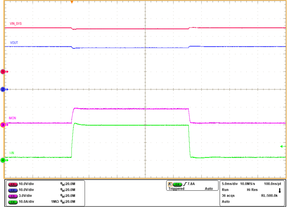 Figure 3-4 IMON Response During Load
Current Step From 2 A to 20 A
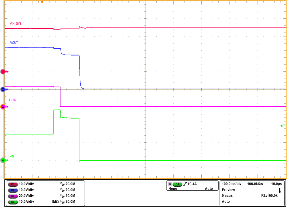 Figure 3-6 Overload Performance
During Load Current Step From 15 A to 28 A
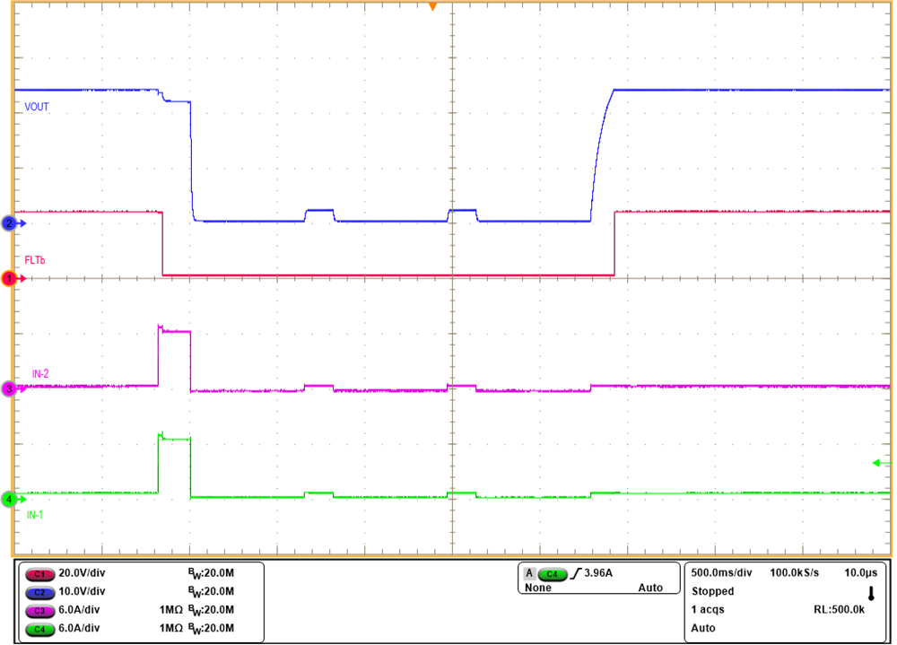 Figure 3-8 Response During Recovery
From Overload Fault
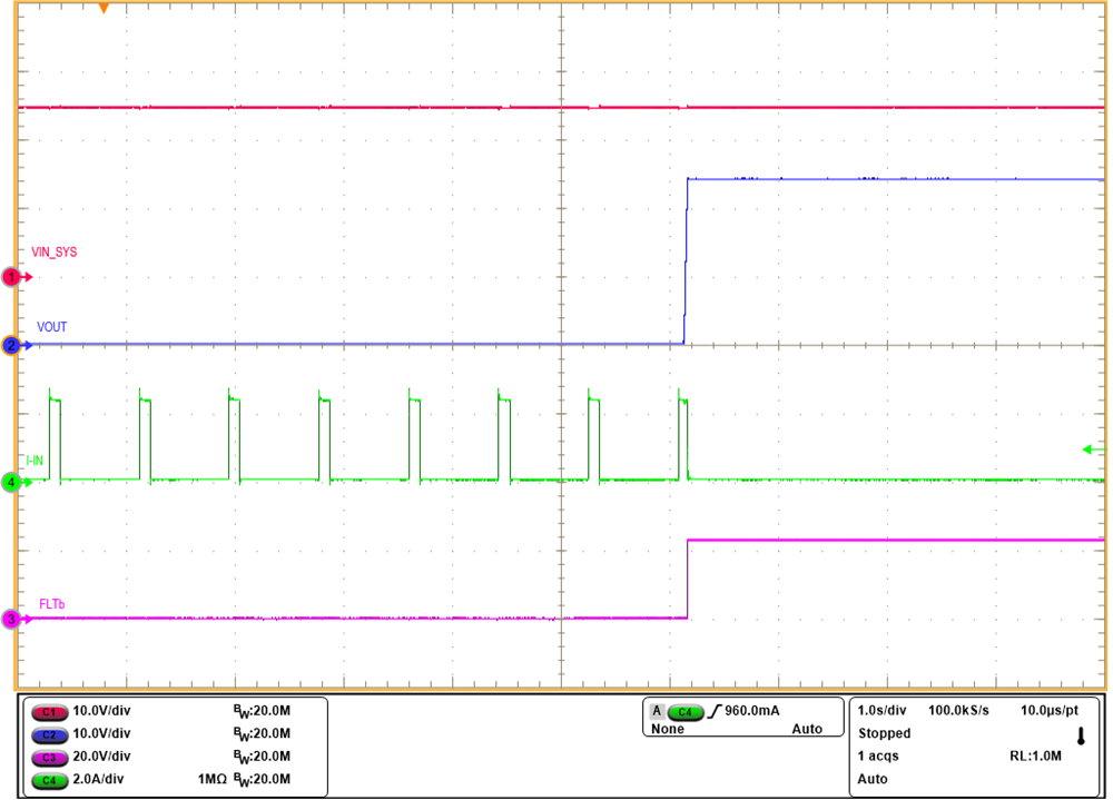 Figure 3-10 Response During Recovery
From Output Short-Circuit
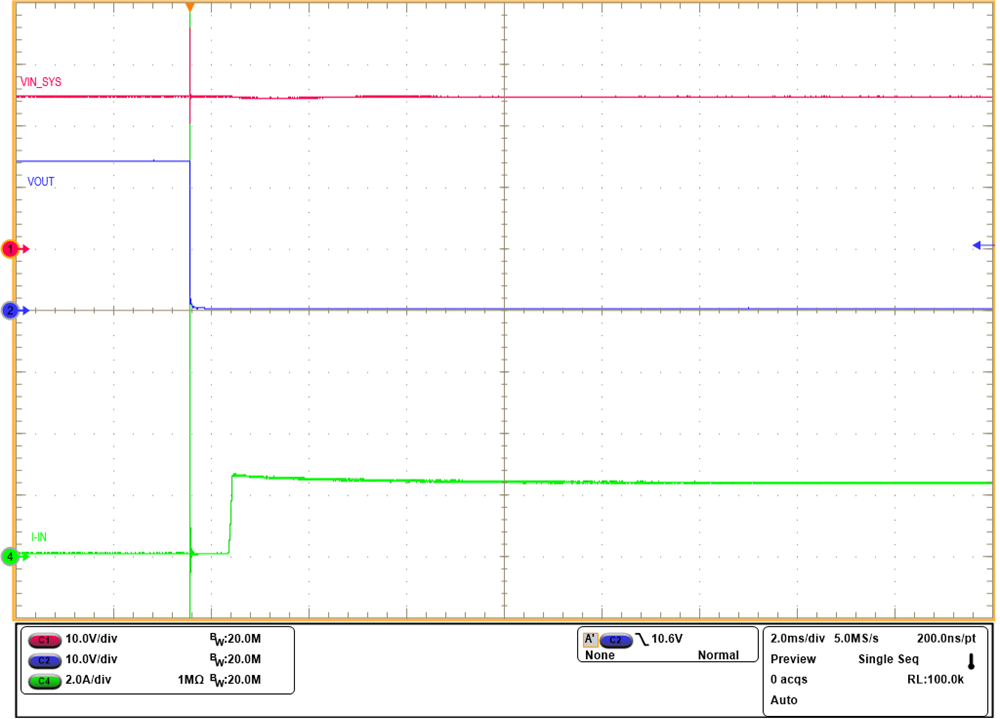 Figure 3-12 Response During Hot-Short
at the Output
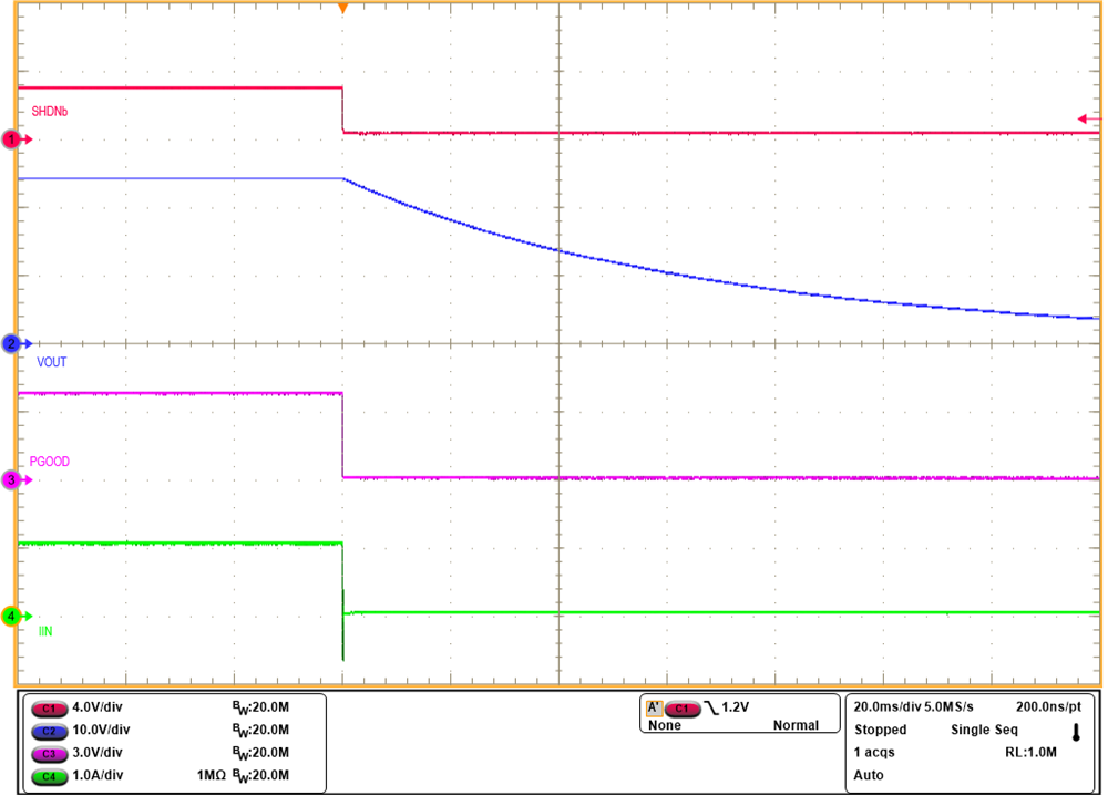 Figure 3-3 Turn-off Control With
SHDN
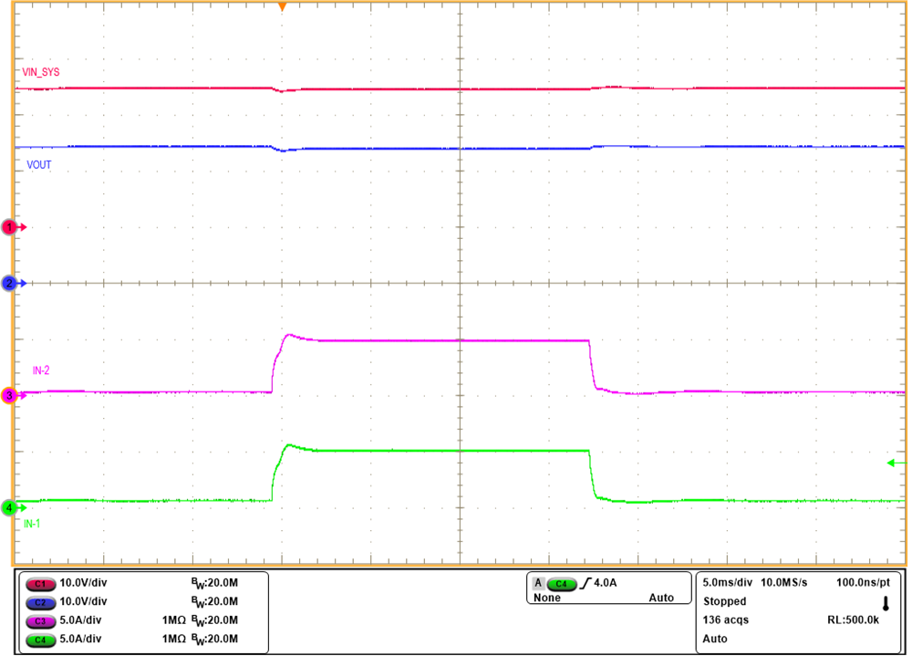 Figure 3-5 Current Sharing Between
Two Devices During Load Current Step from 2 A to 20 A
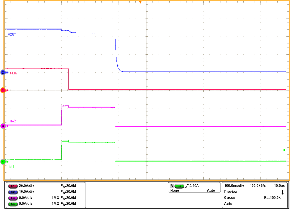 Figure 3-7 Current Sharing Between
Two Devices During Overload Fault
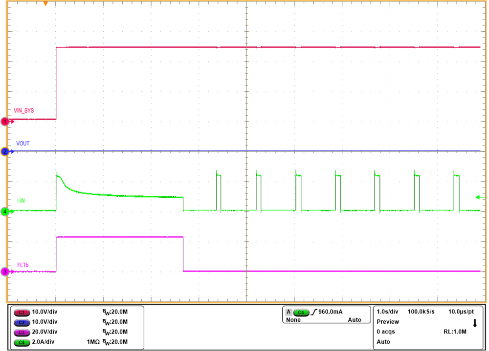 Figure 3-9 Response During Start-up
With Short on Output
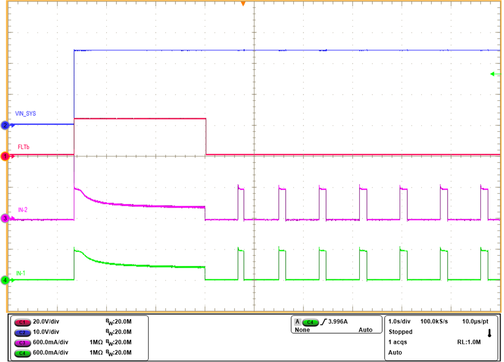 Figure 3-11 Current Sharing Between
Two Devices During Start-up With Short on Output
Figure 3-11 Current Sharing Between
Two Devices During Start-up With Short on Output4 Comparison With the Hot-Swap and ORing Controller Solution
Table 4-1 details the comparison between the solutions.
| Parameter | LM5069 and LM5050 Based Solution | TPS2663 Parallel Configuration | Comments |
|---|---|---|---|
| Input voltage range | 9 V to 80 V, 100 V absolute maximum | 4.5 V to 60 V, 67 V absolute maximum | Higher absolute maximum voltage rating of LM5069 and LM5050 provides flexibility in high voltage applications. |
| Driving large capacitive loads | Yes, using dv/dt
soft-start circuit at the GATE of LM5069 |
Yes |
The thermal regulation loop in the TPS2663 helps to charge unknown capacitive loads as detailed in the Reliable Startup with Large and Unknown Capactive Loads Application Report. |
| MOSFET SOA protection | Yes, through the internal FET power-limiting scheme | Yes, through the internal thermal regulation loop and overtemperature protection | Integration offers accurate FET temperature measurement and reliable protection. External FET solution with the LM5069 always overdesigned to account “factor of safety” for FET SOA. |
| Current limiting (accuracy %) | Yes, (±11.8%) | Yes, (±7%) | Better current limit accuracy with the TPS2663 helps to optimize the input supply size or rating |
| Current monitoring | No | Analog current monitor output with ±6% | |
| Surge protection | Provides only Class-B system performance | The fast recovery feature in the TPS2663 helps to achieve Class-A system performance | The LM5069 solution requires large capacitance at the output to buffer the load during surge, power interruptions for meeting Class-A system performance |
| Supply line transients | Supply line transients cause false trips and often needs trade-off between immunity and short-circuit response | The smart control scheme in the TPS2663 distinguishes real faults from system transients and provides immunity to the transients | |
| Fault status | No | Yes | Fault status output helps to monitor the system status |
|
No. of components |
ICs: LM5069, LM5050 Hot-swap
FET: CSD19502Q5B ORing FETs:
2 × CSD19532Q5B RSENSE: 2 mΩ, 1.5 W COUT: 7 ×
2.2 mF, |
ICs: 4 ×
TPS26631 ORing
FETs: COUT: 3 × 1
mF, |
Only the critical space occupying components are considered. The LM5069 solution requires large output capacitance to meet Class-A system performance. |
| Solution size | 2924 mm2 | 1323 mm2 |
55% reduction in solution size |