SLUS794F November 2007 – April 2016 UCC28070
PRODUCTION DATA.
- 1 Features
- 2 Applications
- 3 Description
- 4 Revision History
- 5 Pin Configuration and Functions
- 6 Specifications
-
7 Detailed Description
- 7.1 Overview
- 7.2 Functional Block Diagram
- 7.3
Feature Description
- 7.3.1 Interleaving
- 7.3.2 Programming the PWM Frequency and Maximum Duty-Cycle Clamp
- 7.3.3 Frequency Dithering (Magnitude and Rate)
- 7.3.4 External Clock Synchronization
- 7.3.5 Multi-phase Operation
- 7.3.6 VSENSE and VINAC Resistor Configuration
- 7.3.7 VSENSE and VINAC Open-Circuit Protection
- 7.3.8 Current Synthesizer
- 7.3.9 Programmable Peak Current Limit
- 7.3.10 Linear Multiplier and Quantized Voltage Feed Forward
- 7.3.11 Enhanced Transient Response (VA Slew-Rate Correction)
- 7.3.12 Voltage Biasing (VCC and VVREF)
- 7.3.13 PFC Enable and Disable
- 7.3.14 Adaptive Soft Start
- 7.3.15 PFC Start-Up Hold Off
- 7.3.16 Output Overvoltage Protection (OVP)
- 7.3.17 Zero-Power Detection
- 7.3.18 Thermal Shutdown
- 7.3.19 Current Loop Compensation
- 7.3.20 Voltage Loop Compensation
- 7.4 Device Functional Modes
-
8 Application and Implementation
- 8.1 Application Information
- 8.2
Typical Application
- 8.2.1 Design Requirements
- 8.2.2
Detailed Design Procedure
- 8.2.2.1 Output Current Calculation
- 8.2.2.2 Bridge Rectifier
- 8.2.2.3 PFC Inductor (L1 and L2)
- 8.2.2.4 PFC MOSFETs (M1 and M2)
- 8.2.2.5 PFC Diode
- 8.2.2.6 PFC Output Capacitor
- 8.2.2.7 Current Loop Feedback Configuration (Sizing of the Current Transformer Turns Ratio and Sense Resistor (RS)
- 8.2.2.8 Current Sense Offset and PWM Ramp for Improved Noise Immunity
- 8.2.3 Application Curves
- 9 Power Supply Recommendations
- 10Layout
- 11Device and Documentation Support
- 12Mechanical, Packaging, and Orderable Information
10 Layout
10.1 Layout Guidelines
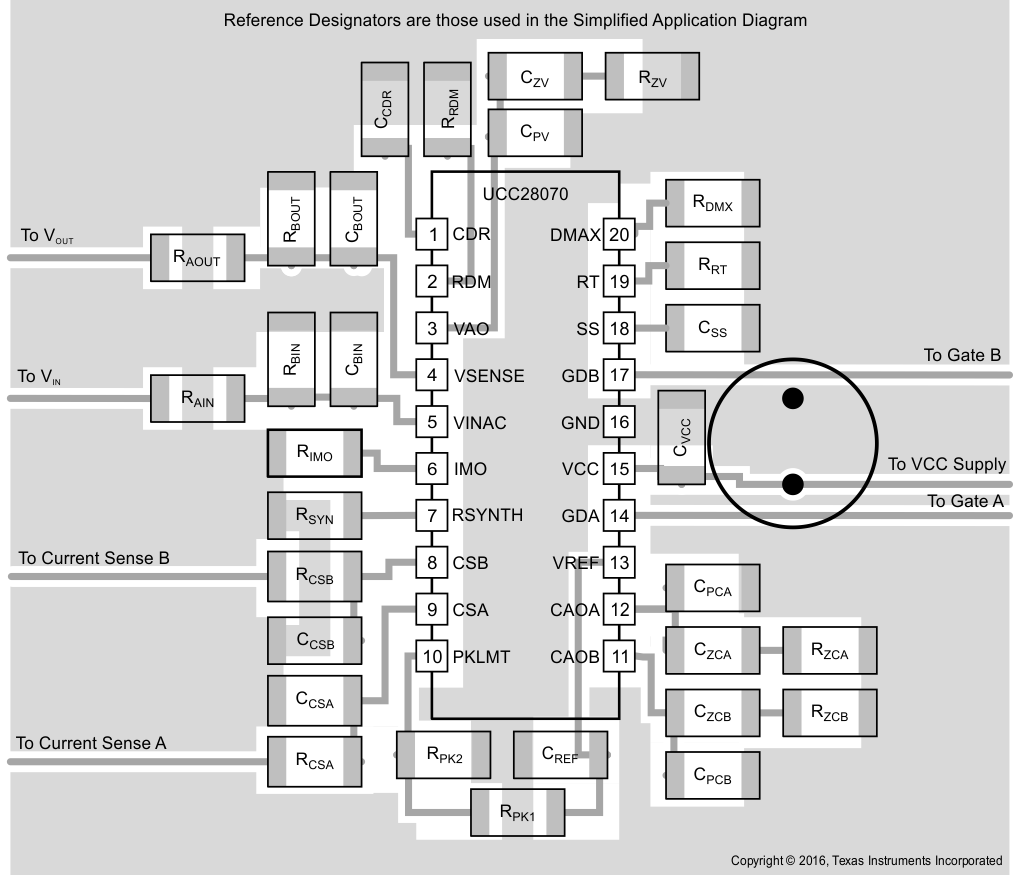
Interleaved PFC techniques dramatically reduce input and output ripple current caused by the PFC boost inductor, which allows the circuit to use smaller and less expensive filters. To maximize the benefits of interleaving, the output filter capacitor should be located after the two phases allowing the current of each phase to be combined together before entering the boost capacitor. Similar to other power management devices, when laying out the PCB it is important to use star grounding techniques and to keep filter and high frequency bypass capacitors as close to device pins and ground as possible. To minimize the possibility of interference caused by magnetic coupling from the boost inductor, the device should be located at least 1 inch away from the boost inductor. TI recommends the device not be placed underneath magnetic elements.
10.2 Layout Example
 Figure 33. Layout Diagram