SLUAAG2 October 2021 UCC28782
4.4 Boost Pin
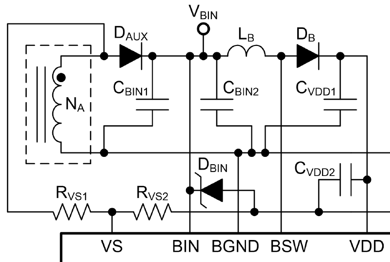
The controller bias power for a wide output voltage range can be simplified with the integrated switching regulator of the UCC28782 and a single auxiliary winding on primary side. The boost conversion mode provides an 18.5-V regulation level for the VDD pin from the rectified auxiliary-winding voltage at the BIN pin.
The boost circuit shown as Figure 4-5, and each component suggestion as below list.
- DAUX: using Schottky diode with 150 V rating for PD application, low Vf is better for low Vo.
- CBIN: if customer does not want to trigger the survival mode, the E-capacitor with larger capacitance is suggested, and it has lower influence with DC bias, and ceramic capacitor still needs to close IC BIN pin.
- DBIN: the BIN pin and BSW pin voltage rating is 30 V, so clamping voltage is suggested 24 V, but it must be higher OVP threshold.
- LB: the 22-μH inductor with higher than 0.4-A saturation current capability and DCR less than 1 Ω resistance is recommended for boost inductor selection.
- DB: the Boost diode is suggested with Schottky diode with 30V rating
 Figure 4-5 Boost Circuit