SLUAA66 May 2020 UCC28740
2 Design Considerations for the Stability
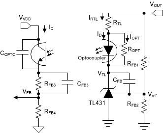
Figure 2 shows the schematic highlighting elements around the TL431 and an optocoupler. At low frequencies, the gain of the TL431 amplifier acts like an integrator with feedback capacitor CFB and resistor RFB1. And, resistor RFB2 provides the correct DC regulation level, but due to the virtual ground at the input of the error amplifier, it does not appear in any of the gain equations.
 Figure 2. Main Feedback and Control Loop
 At mid frequency, the gain of the integrator around the TL431 amplifier reaches unity, and beyond this point, the output voltage signal from the amplifier is attenuated. However, there is always gain from the output voltage to optocoupler diode current due to the connection of the resistor RTL to the power supply output, this is the dominant feedback path in the midband frequencies.
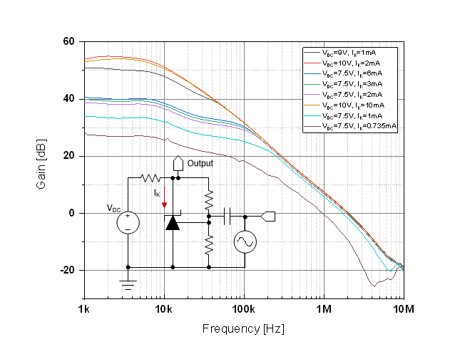
Figure 3 shows the open loop voltage gains of the TL431A (SOT23-3 Package) with different bias conditions, and it’s important to choose a proper pullup resistor since the gain of the TL431A is significantly changed by the pullup resistor. The value of this resistor must be chosen to provide sufficient bias current to the cathode of the TL431A under all operating conditions. Also, notice that the output of the TL431A must be kept above a minimum value required to provide the bias.
Voltage loop stability compensation is applied at the shunt-regulator which drives the opto-coupled feedback signal. The tolerances chosen for the shunt-regulator reference and the sense resistors determine the regulation accuracy.
The TL431A usually requires a minimum bias current of 1 mA to maintain regulation accuracy. Together with the UCC28740 primary-side controller, careful biasing is important to meet standby power loss requirements. The output voltage (VOUT) is set with a resistor divider by RFB1 and RFB2, and it is recommended to use 1% tolerance or better divider resistors. To improve efficiency at light loads consider using larger value resistors. However, if the values are too high, the converter is more susceptible to noise and voltage errors from the Vref input current are noticeable.
 Figure 3. AC Test Results of the TL431A with Different Bias Conditions
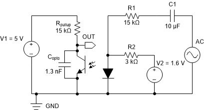
 Figure 4 shows the way the optocoupler can be wired to unveil its pole position. The optocoupler chosen for the EVM (Evaluation Module) design is a LTV-817A of Lite-on, and the V2 source fixes the DC operation point of this common-emitter configuration. For the proper frequency response measurement, 3-kΩ resistor (R2) is used for the DC bias until the collector of the optocoupler measured around 2.5 V, and this is to ensure enough voltage dynamics when the AC sweep will begin. A similar resistor value (15 kΩ) is used for the both Rpullup and R1 to bring the low frequency AC gain to the CTR value in this case.
 Figure 4. Optocoupler Frequency Response Analysis Test Circuit
 The transfer function for this optocoupler frequency response circuit is obtained by calculating the impedance offered by the network placed in the optocoupler diode path, CTR and the common-emitter configuration with Rpullup and Copto.

Developing and arranging Equation 1:

Factoring and rearranging Equation 2, we have:

The locations of the poles are:


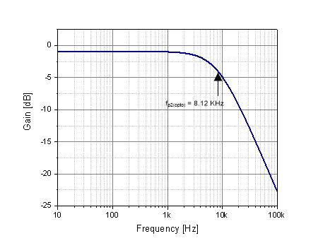
When the optocoupler is connected to FB pin of the UCC28740, it will introduce a pole (fp2(opto)) due to Copto coupling with the pull-up resistor (or the pull down in a common-collector configuration). fp2(opto) will affect the total system stability, and the contribution of Copto should be considered for the stable operation. Also, note that changing the DC operating point (different Vce of the optocoupler) does not affect the pole position. Figure 5 shows the frequency response of LTV-817A (Lite-on) optocoupler, and fp2(opto) measured to be 8.12 kHz at -3 dB gain attenuation as it is calculated in Equation 5.
 Figure 5. Frequency Response of LTV-817A Optocoupler
 A capacitor (CP) can be added in parallel with the optocoupler in the primary side to adjust the location of fp2(opto). When the optocoupler capacitor couples to a capacitor (CP), the new pole is shifted to

Therefore, once a capacitor (CP) is known, it is needed to calculate the new pole frequency, and the new pole frequency will be lower compared to fp2(opto) with this approach. The solution is to explore a new pole for the proper gain and phase margins.
The control law of the UCC28740 combines frequency with primary peak-current amplitude modulation and provides a wide dynamic operating range of output power which allows the power supply designer to easily achieve less than 30 mW standby power dissipation using a standard shunt-regulator and optocoupler. For a target of less than 10 mW standby power, careful loss-management design with a low power regulator and high CTR optocoupler is required.
In Figure 2, the transfer function from VTL to VFB is obtained by calculating the impedance offered by the network placed in the optocoupler diode path on the primary side with CTR.

The location of the zero is determined by:

fz can be extracted from Equation 8 to obtain (considering CFB3=47 nF, RFB3=196k Ω, RFB4=22 kΩ)

Also, the locations of the first pole and the second pole are determined by:

fp1 and fp2 can be extracted from Equation 10 (considering Copto=1.3 nF)


Since the location of the both fz and fp1 is about 17 Hz as shown in Equation 9 and Equation 11, fp2 plays the role of the dominant pole in the system. To make the system stable, the crossover frequency should be less than fp2. If fp2 is less than the crossover frequency, the gain falls at a rate of -40 dB/decade, and the system will be unstable in this case.