SLUA749A July 2015 – May 2016 BQ76920 , BQ76930 , BQ76940
6 FET Drive
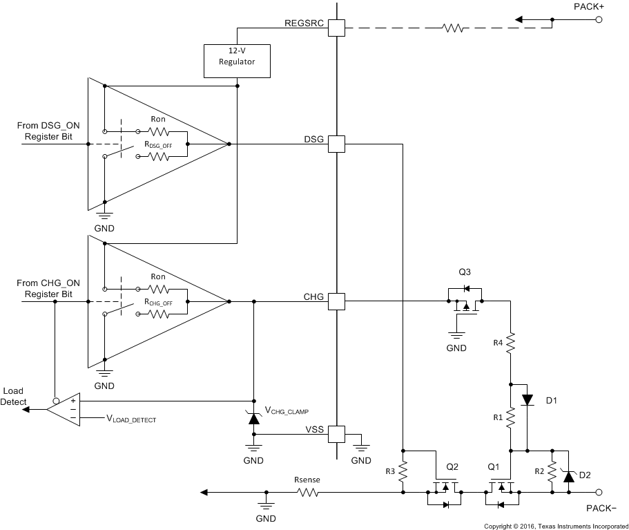
The bq769x0 family has FET control outputs referenced to VSS as described in the datasheet. The CHG and DSG outputs are powered from a 12-V supply regulated from the REGSRC supply. When high, the outputs will be 12 V nominal when the REGSRC supply voltage is sufficient. If the voltage drops below the regulation point the CHG and DSG output voltages will also drop. These outputs may be used to drive small to medium low-side protection FETs. A typical circuit is shown in Figure 9. When large FET arrays are used, a driver will be needed, the ground referenced CHG and DSG outputs should be easy to interface to a driver. A high impedance driver is recommended for the charge driver due to the high resistance pulldown of the CHG pin.
 Figure 9. Typical Low-Side FET Connection
 The DSG output can connect directly to the low side N-channel FET gate when it is suitable since the driver has an internal resistance to limit the switching speed of the FET. Pull-down resistance of the DSG output is shown in the datasheet and is typically 2.5 kΩ. The pull-up resistance may be calculated from the rise time conditions in the datasheet and is approximately 5 kΩ. Increasing the load current or the FET gate capacitance will cause the driver to switch more slowly. In some cases an additional resistance may be desired between the DSG pin and the discharge FET gate, this will slow the discharge gate switching. When multiple FETs are used, a small resistor to the gate of each FET may be desired, check with your FET supplier. Switching speed will slow with multiple FETs due to the added capacitance. When faster switching is needed a driver will be needed for the FET gate.
The CHG pin must be connected to the charge FET gate through a circuit to allow the charge FET to operate properly in several phases of operation. The typical circuit is shown in the datasheet and in Figure 9. CHG pin pull-down resistance is 1 MΩ nominal, pull-up resistance can be calculated from the rise time and is approximately 5 kΩ.
When the battery is in a normal state and has both the Q1 and Q2 FETs ON, it is desirable to have most of the CHG pin voltage available on the gate of Q2 to maintain a low resistance in the FET. Q3 will be on with a low resistance. D1 will provide a fixed drop ‘shorting’ R1. A voltage divider will be created by R4 and R2. R2 should be large and R4 small so that most of the CHG pin voltage is applied to the gate. R2 may be 1 MΩ typical while R4 may be 1 kΩ.
When the CHG pin turns off, it will pull down the Q1 charge FET gate through Q3 body diode, R4, and R1. R2 also pulls down the gate and when the charger pushes the PACK- voltage below battery-, R2 keeps Q1 off. Q3 is off and allows the Q1 gate and source to fall to a large voltage below the IC VSS at the battery- voltage.
When the CHG output turns on CHG and Q3 drain will try to go to approximately 12 V. If the battery had been discharged 15 V below the charger voltage, there would be a 27 V difference between the Q1 source and the Q3 drain voltage. D2 avoids a damaging voltage from being applied to the Q1 gate if the FET does not turn on fast enough to limit the gate voltage. R4 will drop some voltage but may be considered optional since Q3 would limit the current when the CHG pin voltage pulled down sufficiently. D2 should be selected so that it does not conduct when Q1 is on with PACK- at the battery- voltage but protects Q1 against transients exceeding the VGS maximum limits. For low voltage batteries, D2 may not be required.
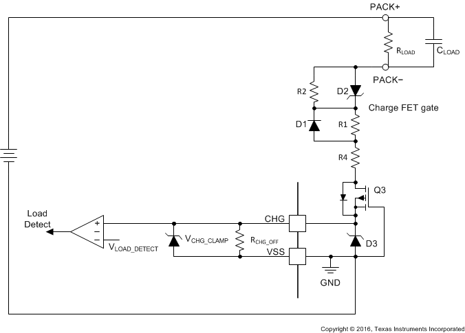
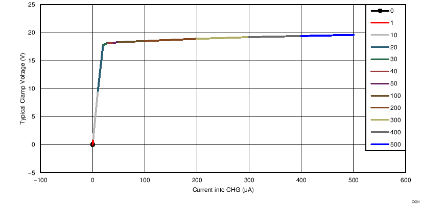
When the discharge FET is off and a load is applied to the battery, PACK- will pull up toward PACK+. Normally in this situation the system will also turn off the CHG driver. In this condition the circuit behavior may be easier to visualize if re-drawn with the power FETs removed as in Figure 10. PACK- may be the same voltage as PACK+ if RLOAD is small. D2 conducts and protects the Q1 gate from excessive voltage. The CHG pin voltage will rise to the VCHG_CLAMP voltage. D1 blocks current flow so the voltage between D2 and the CHG pin is dropped across R1 and R4. R4 is small, so R1 must be large to limit current into the CHG pin. Q3 will be on in this condition. The designer may note that the datasheet test current CHG sink current is 500 µA, but the maximum VCHG_CLAMP at this test current is 22 V maximum and would exceed the VGS maximum of most FETs used for Q3. With a 50-V difference between the PACK- and CHG and a 1-MΩ resistance the current into CHG would be approximately 50 µA. The VCHG_CLAMP is lower at lower current as shown in Figure 11, however, without a maximum voltage at a similar test condition designers may chose to implement their own known clamp as shown at D3. The D3 clamp value may be in the 15- to 18-V range so that it protects the Q3 VGS maximum limit but does not conduct at normal CHG output levels. As noted in a previous paragraph, a low voltage battery pack may not need a D2 zener to prevent excessive positive VGS on Q1. The same pack low-voltage pack may not need D2 to prevent excessive negative VGS. Current may be further reduced or the designer may consider removing R1 and D1 since R2 could provide sufficient current limit. R1 and R2 should generally be large to limit the leakage current when the load remains on the PACK with the FETs off.
 Figure 10. CHG Circuit With Load Applied
  Figure 11. CHG Pin Typical Clamp Voltage
 Turn off of the CHG FET will be slow with the high resistance of the CHG pin, its path resistance and the gate-source resistor. For many systems the charge current is much lower than the discharge current and the slow switching from this high resistance allows the charge FET to switch within the safe operating area of the FET. Systems which have higher charge currents or parallel FETs may require a driver. As with the circuit described above, the driver will need to float from possibly a large negative voltage up to the PACK positive voltage and limit current into the CHG pin when high. It will need a power supply, a level shifter and should reference PACK- to keep the FET off when the charger voltage is greater than the battery voltage.