-
TPA2012D2 2.1-W/Channel Stereo Filter-Free Class-D Audio Power Amplifier
- 1 Features
- 2 Applications
- 3 Description
- 4 Revision History
- 5 Device Comparison Table
- 6 Pin Configuration and Functions
- 7 Specifications
- 8 Parameter Measurement Information
- 9 Detailed Description
- 10Application and Implementation
- 11Power Supply Recommendations
- 12Layout
- 13Device and Documentation Support
- 14Mechanical, Packaging, and Orderable Information
- IMPORTANT NOTICE
TPA2012D2 2.1-W/Channel Stereo Filter-Free Class-D Audio Power Amplifier
1 Features
- Output Power By Package:
- WQFN:
- 2.1 W/Ch Into 4 Ω at 5 V
- 1.4 W/Ch Into 8 Ω at 5 V
- 720 mW/Ch Into 8 Ω at 3.6 V
- DSBGA:
- 1.2 W/Ch Into 4 Ω at 5 V
(Thermally Limited) - 1.3 W/Ch Into 8 Ω at 5 V
- 720 mW/Ch Into 8 Ω at 3.6 V
- 1.2 W/Ch Into 4 Ω at 5 V
- WQFN:
- Only Two External Components Required
- Power Supply Range: 2.5 V to 5.5 V
- Independent Shutdown Control for Each Channel
- Selectable Gain of 6, 12, 18, and 24 dB
- Internal Pulldown Resistor on Shutdown Pins
- High PSRR: 77 dB at 217 Hz
- Fast Start-Up Time (3.5 ms)
- Low Supply Current
- Low Shutdown Current
- Short-Circuit and Thermal Protection
- Space-Saving Packages
- 2.01-mm × 2.01-mm NanoFree™ DSBGA (YZH)
- 4-mm × 4-mm Thin WQFN (RTJ) With PowerPAD™
2 Applications
- Wireless or Cellular Handsets and PDAs
- Portable DVD Players
- Notebook PCs
- Portable Radios
- Portable Gaming
- Educational Toys
- USB Speakers
3 Description
The TPA2012D2 is a stereo, filter-free, Class-D audio amplifier (Class-D amp) available in a DSBGA or WQFN package. The TPA2012D2 only requires two external components for operation.
The TPA2012D2 features independent shutdown controls for each channel. The gain can be selected to 6, 12, 18, or 24 dB using the G0 and G1 gain select pins. High PSRR and differential architecture provide increased immunity to noise and RF rectification. In addition to these features, a fast start-up time and small package size make the TPA2012D2 class-D amp an ideal choice for both cellular handsets and PDAs.
The TPA2012D2 is capable of driving 1.4 W/Ch at
5 V or 720 mW/Ch at 3.6 V into 8 Ω. The TPA2012D2 is also capable of driving 4 Ω. The TPA2012D2 is thermally limited in DSBGA and may not achieve
2.1 W/Ch for 4 Ω. The maximum output power in the DSBGA is determined by the ability of the circuit board to remove heat. Figure 33 shows thermally limited region of the DSBGA in relation to the WQFN package. The TPA2012D2 provides thermal and short-circuit protection.
Device Information(1)
| PART NUMBER | PACKAGE | BODY SIZE (NOM) |
|---|---|---|
| TPA2012D2 | DSBGA (16) | 2.01 mm × 2.01 mm |
| WQFN (20) | 4.00 mm × 4.00 mm |
- For all available packages, see the orderable addendum at the end of the data sheet.
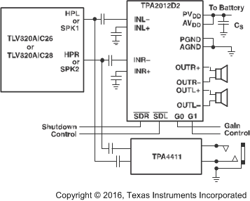
Simplified Application Schematic
4 Revision History
Changes from E Revision (September 2016) to F Revision
- Switched the BODY SIZE values in the Device Information table: DSBGA From: 4.00 mm × 4.00 mm To: 2.01 mm × 2.01 mm and WQFN From: 2.01 mm × 2.01 mm To: 4.00 mm × 4.00 mmGo
Changes from D Revision (June 2008) to E Revision
- Added ESD Ratings table, Feature Description section, Device Functional Modes, Application and Implementation section, Power Supply Recommendations section, Layout section, Device and Documentation Support section, and Mechanical, Packaging, and Orderable Information sectionGo
- Deleted Available-Options table; see POA at the end of the data sheetGo
- Deleted previous application schematics: Typical Application Circuit (previously Figure 33), TPA2012D2 Application Schematic With Differential Input and Input Capacitors (previously Figure 34), and TPA2012D2 Application Schematic With Single-Ended Input (previously Figure 35)Go
5 Device Comparison Table
| DEVICE NO. | SPEAKER AMP TYPE | SPECIAL FEATURE | OUTPUT POWER (M) | PSRR (dB) |
|---|---|---|---|---|
| TPA2012D2 | Class D | — | 2.1 | 71 |
| TPA2016D2 | Class D | AGC/DRC | 2.8 | 80 |
| TPA2026D2 | Class D | AGC/DRC | 3.2 | 80 |
6 Pin Configuration and Functions
Pin Functions
| PIN | I/O | DESCRIPTION | ||
|---|---|---|---|---|
| NAME | DSBGA | WQFN | ||
| AGND | C3 | 18 | I | Analog ground |
| AVDD | D2 | 9 | I | Analog supply (must be same voltage as PVDD) |
| G0 | C2 | 15 | I | Gain select (LSB) |
| G1 | B2 | 1 | I | Gain select (MSB) |
| INL– | B1 | 19 | I | Left channel negative input |
| INL+ | A1 | 20 | I | Left channel positive input |
| INR– | C1 | 17 | I | Right channel negative input |
| INR+ | D1 | 16 | I | Right channel positive input |
| NC | — | 6, 10 | — | No internal connection |
| OUTL– | A4 | 5 | O | Left channel negative differential output |
| OUTL+ | A3 | 2 | O | Left channel positive differential output |
| OUTR– | D4 | 11 | O | Right channel negative differential output |
| OUTR+ | D3 | 14 | O | Right channel positive differential output |
| PGND | C4 | 4, 12 | I | Power ground |
| PVDD | A2 | 3, 13 | I | Power supply (must be same voltage as AVDD) |
| SDL | B4 | 7 | I | Left channel shutdown terminal (active low) |
| SDR | B3 | 8 | I | Right channel shutdown terminal (active low) |
| Thermal Pad | — | — | — | Connect the thermal pad of WQFN package to PCB GND |
7 Specifications
7.1 Absolute Maximum Ratings
over operating free-air temperature range (unless otherwise noted)(1)| MIN | MAX | UNIT | ||
|---|---|---|---|---|
| Supply voltage, VSS (AVDD, PVDD) | Active mode | –0.3 | 6 | V |
| Shutdown mode | –0.3 | 7 | ||
| Input voltage, VI | –0.3 | VDD + 0.3 | V | |
| Continuous total power dissipation | See Dissipation Rating Table | |||
| Operating junction temperature, TJ | –40 | 150 | °C | |
| Storage temperature, Tstg | –65 | 150 | °C | |
7.2 ESD Ratings
| VALUE | UNIT | |||
|---|---|---|---|---|
| V(ESD) | Electrostatic discharge | Human-body model (HBM), per ANSI/ESDA/JEDEC JS-001(1) | ±2000 | V |
| Charged-device model (CDM), per JEDEC specification JESD22-C101(2) | ±1500 | |||
7.3 Recommended Operating Conditions
over operating free-air temperature range (unless otherwise noted)| MIN | MAX | UNIT | ||
|---|---|---|---|---|
| VSS | Supply voltage, AVDD, PVDD | 2.5 | 5.5 | V |
| VIH | High-level input voltage, SDL, SDR, G0, G1 | 1.3 | V | |
| VIL | Low-level input voltage, SDL, SDR, G0, G1 | 0.35 | V | |
| TA | Operating free-air temperature | –40 | 85 | °C |
7.4 Thermal Information
| THERMAL METRIC(1) | TPA2012D2 | UNIT | ||
|---|---|---|---|---|
| YZH (DSBGA) | RTJ (WQFN) | |||
| 16 PINS | 20 PINS | |||
| RθJA | Junction-to-ambient thermal resistance | 71.4 | 34.6 | °C/W |
| RθJC(top) | Junction-to-case (top) thermal resistance | 0.4 | 34.3 | °C/W |
| RθJB | Junction-to-board thermal resistance | 14 | 11.5 | °C/W |
| ψJT | Junction-to-top characterization parameter | 1.8 | 0.4 | °C/W |
| ψJB | Junction-to-board characterization parameter | 13.3 | 11.6 | °C/W |
| RθJC(bot) | Junction-to-case (bottom) thermal resistance | — | 3.2 | °C/W |
7.5 Electrical Characteristics
TA = 25°C (unless otherwise noted)| PARAMETER | TEST CONDITIONS | MIN | TYP | MAX | UNIT | ||
|---|---|---|---|---|---|---|---|
| |VOO| | Output offset voltage (measured differentially) | Inputs ac grounded, AV = 6 dB, VDD = 2.5 to 5.5 V | 5 | 25 | mV | ||
| PSRR | Power supply rejection ratio | VDD = 2.5 to 5.5 V | –75 | –55 | dB | ||
| Vicm | Common-mode input voltage | 0.5 | VDD – 0.8 | V | |||
| CMRR | Common-mode rejection ration | Inputs shorted together, VDD = 2.5 to 5.5 V | –69 | –50 | dB | ||
| |IIH| | High-level input current | VDD = 5.5 V, VI = VDD | 50 | µA | |||
| |IIL| | Low-level input current | VDD = 5.5 V, VI = 0 V | 5 | µA | |||
| IDD | Supply current | VDD = 5.5 V, no load or output filter | 6 | 9 | mA | ||
| VDD = 3.6 V, no load or output filter | 5 | 7.5 | |||||
| VDD = 2.5 V, no load or output filter | 4 | 6 | |||||
| Shutdown mode | 1.5 | µA | |||||
| rDS(on) | Static drain-source on-state resistance | VDD = 5.5 V | 500 | mΩ | |||
| VDD = 3.6 V | 570 | ||||||
| VDD = 2.5 V | 700 | ||||||
| Output impedance in shutdown mode | V(SDR, SDL)= 0.35 V | 2 | kΩ | ||||
| f(sw) | Switching frequency | VDD = 2.5 V to 5.5 V | 250 | 300 | 350 | kHz | |
| Closed-loop voltage gain | G0, G1 = 0.35 V | 5.5 | 6 | 6.5 | dB | ||
| G0 = VDD, G1 = 0.35 V | 11.5 | 12 | 12.5 | ||||
| G0 = 0.35 V, G1 = VDD | 17.5 | 18 | 18.5 | ||||
| G0, G1 = VDD | 23.5 | 24 | 24.5 | ||||
| OPERATING CHARACTERISTICS, RL = 8 Ω | |||||||
| PO | Output power (per channel) | RL = 8 Ω | VDD = 5 V, f = 1 kHz, THD = 10% |
1.4 | W | ||
| VDD = 3.6 V, f = 1 kHz, THD = 10% |
0.72 | ||||||
| RL = 4 Ω | VDD = 5 V, f = 1 kHz, THD = 10% |
2.1 | |||||
| THD+N | Total harmonic distortion plus noise | PO = 1 W, VDD = 5 V, AV = 6 dB, f = 1 kHz | 0.14% | ||||
| PO = 0.5 W, VDD = 5 V, AV = 6 dB, f = 1 kHz | 0.11% | ||||||
| Channel crosstalk | f = 1 kHz | –85 | dB | ||||
| kSVR | Supply ripple rejection ratio | VDD = 5 V, AV = 6 dB, f = 217 Hz | –77 | dB | |||
| VDD = 3.6 V, AV = 6 dB, f = 217 Hz | –73 | ||||||
| CMRR | Common mode rejection ratio | VDD = 3.6 V, VIC = 1 Vpp, f = 217 Hz | –69 | dB | |||
| Input impedance | Av = 6 dB | 28.1 | kΩ | ||||
| Av = 12 dB | 17.3 | ||||||
| Av = 18 dB | 9.8 | ||||||
| Av = 24 dB | 5.2 | ||||||
| Start-up time from shutdown | VDD = 3.6 V | 3.5 | ms | ||||
| Vn | Output voltage noise | VDD = 3.6 V, f = 20 to 20 kHz, inputs are ac grounded, AV = 6 dB |
No weighting | 35 | µV | ||
| A weighting | 27 | ||||||
7.6 Dissipation Rating Table
| PACKAGE | TA = 25°C POWER RATING(1) |
DERATING FACTOR |
TA = 75°C POWER RATING |
TA = 85°C POWER RATING |
|---|---|---|---|---|
| RTJ | 5.2 W | 41.6 mW/°C | 3.12 W | 2.7 W |
| YZH | 1.2 W | 9.12 mW/°C | 690 mW | 600 mW |
7.7 Typical Characteristics
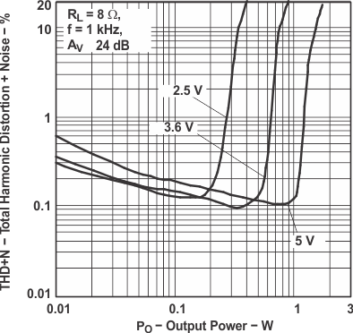 Figure 1. Total Harmonic Distortion
vs Output Power
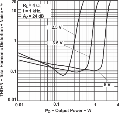 Figure 3. Total Harmonic Distortion
vs Output Power
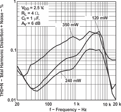 Figure 5. Total Harmonic Distortion vs Frequency
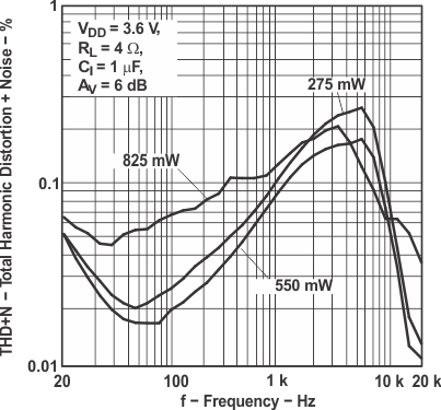 Figure 7. Total Harmonic Distortion vs Frequency
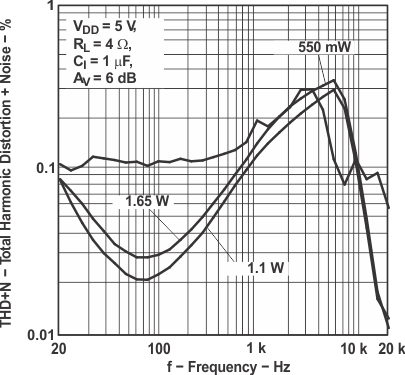 Figure 9. Total Harmonic Distortion vs Frequency
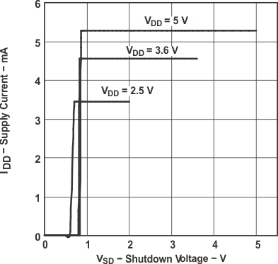 Figure 11. Supply Current vs Shutdown Voltage
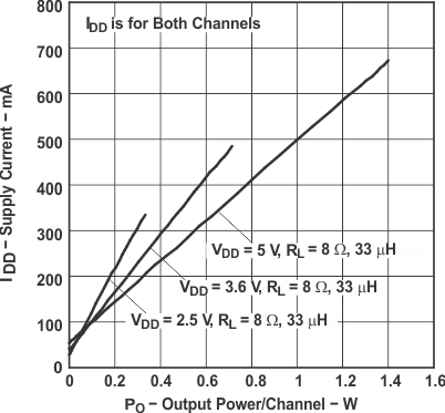 Figure 13. Supply Current vs Output Power
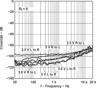 Figure 15. Crosstalk vs Frequency
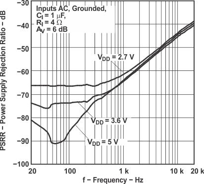 Figure 17. Power Supply Rejection Ratio
vs Frequency
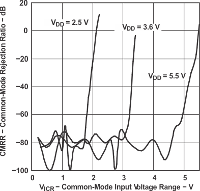 Figure 19. Common-Mode Rejection Ratio
vs Common-Mode Input Voltage
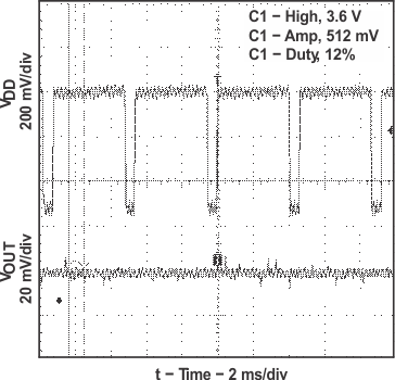 Figure 21. GSM Power Supply Rejection vs Time
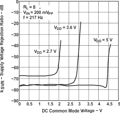 Figure 23. Supply Voltage Rejection Ratio
vs DC Common-Mode Voltage
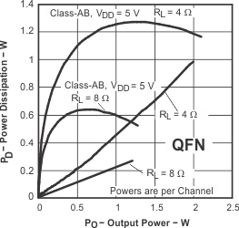 Figure 25. Power Dissipation vs Output Power
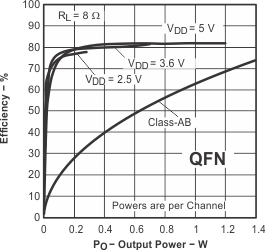 Figure 27. Efficiency vs Output Power
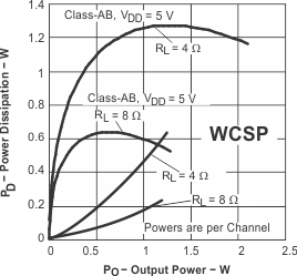 Figure 29. Power Dissipation vs Output Power
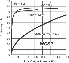 Figure 31. Efficiency vs Output Power
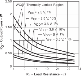 Figure 33. Output Power vs Load Resistance
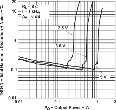 Figure 2. Total Harmonic Distortion
vs Output Power
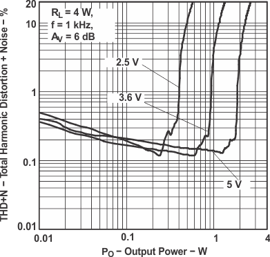 Figure 4. Total Harmonic Distortion
vs Output Power
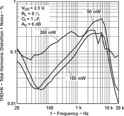 Figure 6. Total Harmonic Distortion vs Frequency
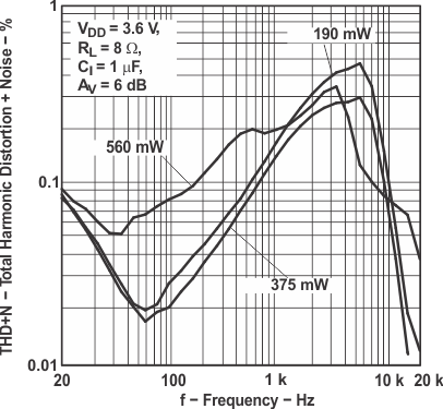 Figure 8. Total Harmonic Distortion vs Frequency
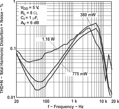 Figure 10. Total Harmonic Distortion vs Frequency
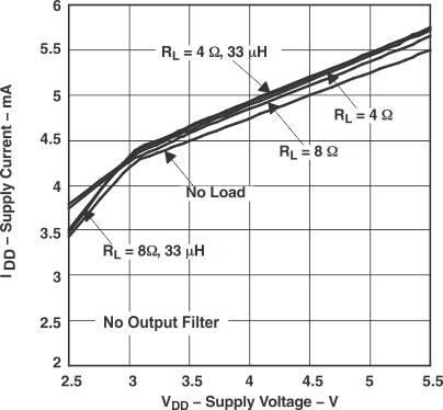 Figure 12. Supply Current vs Supply Voltage
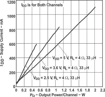 Figure 14. Supply Current vs Output Power
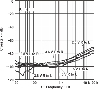 Figure 16. Crosstalk vs Frequency
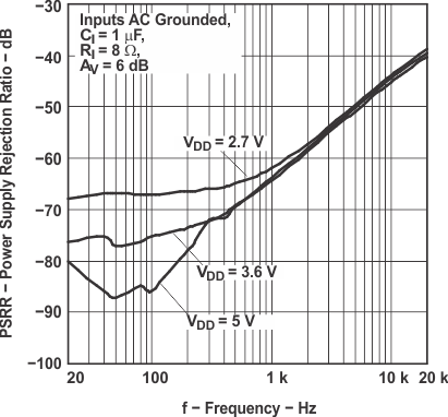 Figure 18. Power Supply Rejection Ratio
vs Frequency
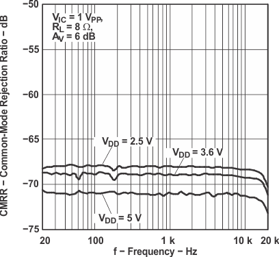 Figure 20. Common-Mode Rejection Ratio
vs Frequency
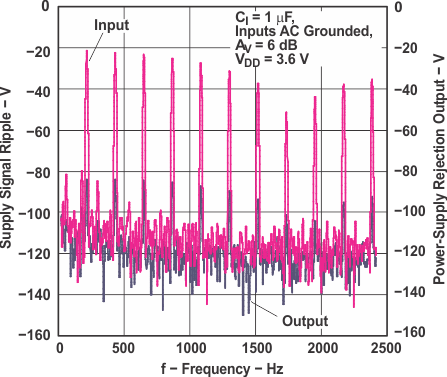 Figure 22. Power Supply Rejection vs Frequency
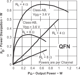 Figure 24. Power Dissipation vs Output Power
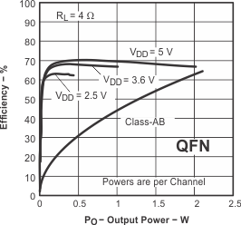 Figure 26. Efficiency vs Output Power
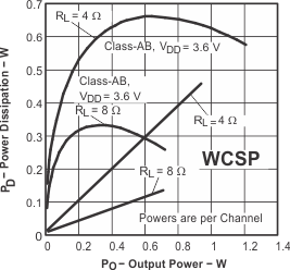 Figure 28. Power Dissipation vs Output Power
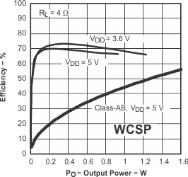 Figure 30. Efficiency vs Output Power
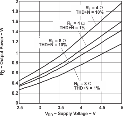 Figure 32. Output Power vs Supply Voltage