SLLA572 December 2021 SN65HVD888 , THVD1505
2 Test Cases
Test Case 1: A-A and B-B correct connection
Two half-duplex RS-485 EVMs are used in this test. The 5-V supply is individually supplied to each board. THVD1550 (regular non-polarity free RS-485 transceiver) is populated with a 120-Ω termination on board 1 as shown in Figure 2-1. This board is set as the leading node in the test, where the DE and D pins (pin 2 and pin 3) are high and the REB pin (pin 1) is low. On board 2, THVD1505 (polarity free RS-485 transceiver) is populated with a 120-Ω termination. This board is configured with the D pin high and the DE and REB pin low to make it function as the follower in the test. The receiver output R pin is biased with a 10k-Ω pull-down resistor. The wires between these two boards are connected normally, meaning A (pin 7) is wired to A and B (pin 6) is wired to B between the two boards.
In this test, THVD1550 is used to set the bus polarity. After board 1 is powered on, board 2 is turned on a few seconds later. The bus waveforms (A: purple curve; B: green curve) and R (blue curve) of THVD1505 in Figure 2-2 show that THVD1505 detects the bus polarity correctly after being powered up. Since the bus bias is positive, the correct output at R is generated to be a logic high. Similar results are obtained with SN65HVD888 deployed on Board 2, as shown in Figure 2-3.
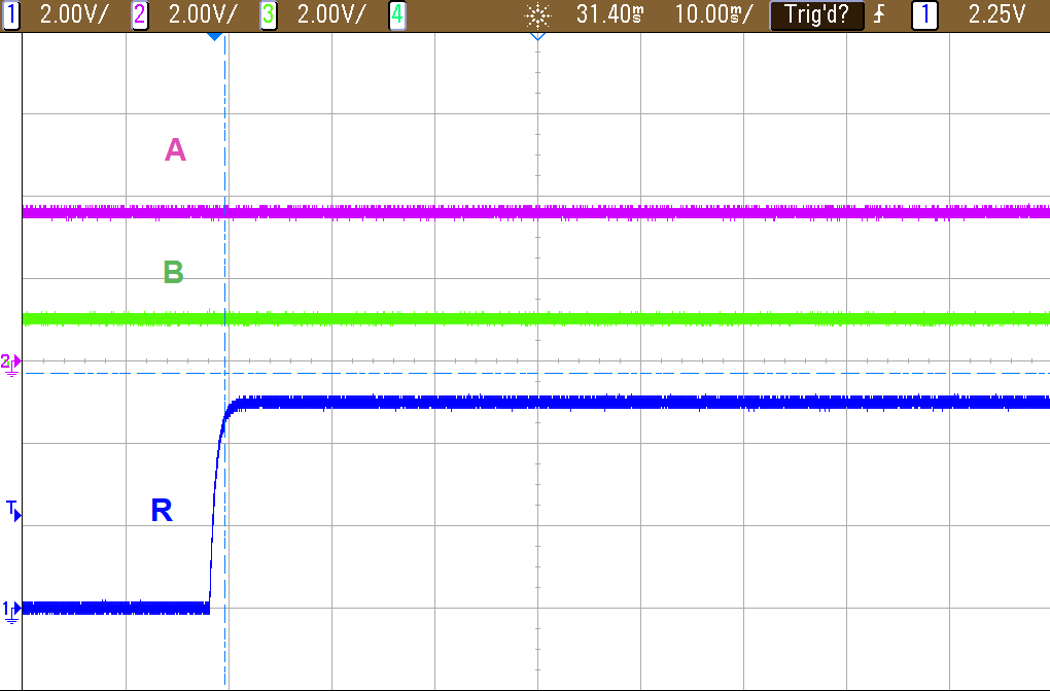 Figure 2-2 THVD1505 Powered Up with
Correct Wiring
 Figure 2-3 SN65HVD888 Powered Up with
Correct Wiring
Figure 2-3 SN65HVD888 Powered Up with
Correct WiringTest Case 2: A-B and B-A Miswiring Connection
In this test, two boards are configured in a similar way as test case #1. However, the wire connections are mis-wired (Figure 2-4). To be more specific, the pin A of board 1 is wired to the pin B of board 2, while pin B of board 1 is wired to the pin A of board 2.
Comparing to the results of Test case #1, Figure 2-5 shows that the voltage of the R pin (blue curve) of THVD1505 follows the rail during power ramping up. As the supply is high enough to fully turn on the device, the receiver output becomes low responding to the negative bus bias (the voltage of pin A of THVD1505 is lower than that of pin B). Nevertheless, the device keeps checking the bus polarity as it is powered up. After a certain time (fail-safe time tFS), the receiver recognizes the bus polarity and corrects itself to match that. Therefore, the R pin voltage flips from low to high. Similar results are observed with SN65HVD888 on board 2, as shown in Figure 2-6. The longer timing difference shown in Figure 2-6 is due to the longer fail-safe time of SN65HVD888.
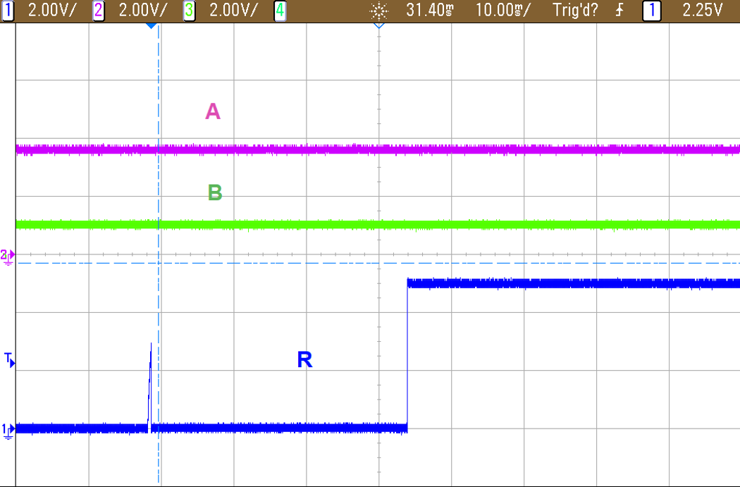 Figure 2-5 THVD1505 Powered Up with
Mis-wiring
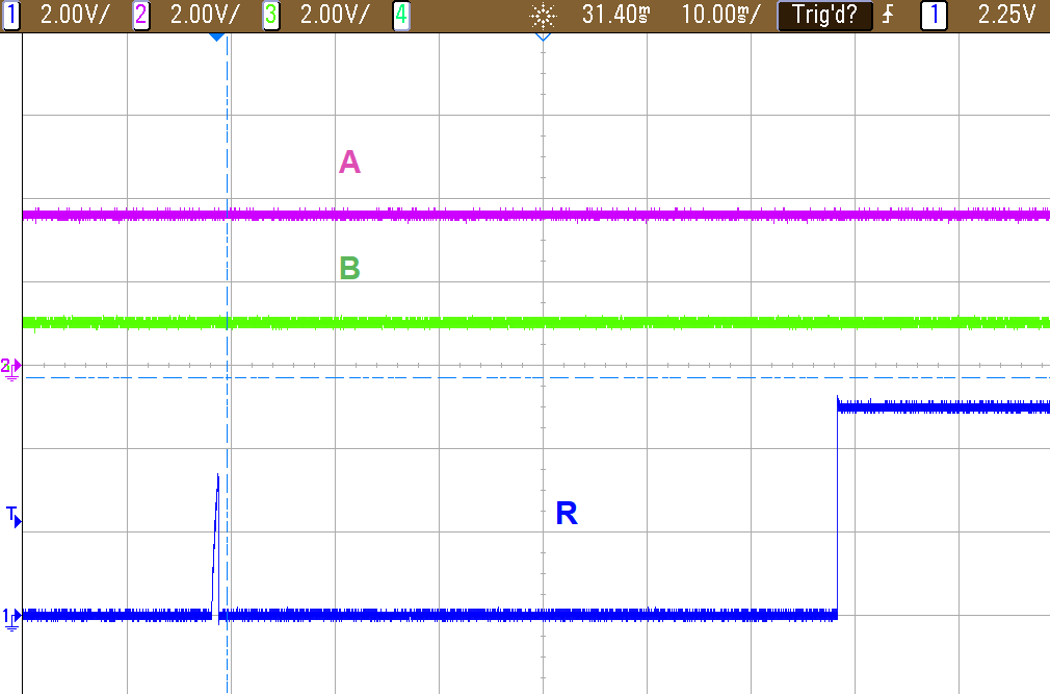 Figure 2-6 SN65HVD888 Powered Up with
Mis-wiring
Figure 2-6 SN65HVD888 Powered Up with
Mis-wiringTest Case 3: A-B and B-A miswiring connection with drivers on
This break-the-part test shows what could happen if the driver of the polarity-free transceiver is turned on before the polarity information has been processed by the device.
In this test, board 1 is populated with THVD1550, while the enable pins are set as before (the DE pin and D pin are high, the REB pin low) (Figure 2-7). Please note that both boards are not terminated, for better demonstrating the devices’ behavior in this problematic setup. Since it is supposed to drive the bus, the DE and D pins are high and the REB pin is low as board 1. Similarly, the wire connections are mis-wired (pin A of board 1 is wired to pin B of board 2, pin B of board 1 is wired to pin A of board 2).
In Figure 2-8, the driver of THVD1505 is immediately turned on as the device is powered up. Same as the last two tests, the waveforms are A: purple curve; B: green curve and R: blue curve of THVD1505. However, by default the device’s polarity is opposite to the bus or the polarity of THVD1550. Two drivers with the same input (logic high) drive the bus oppositely, causing the bus voltage to stay somewhere around half of Vcc. Please note that depending on the drive strength of the two drivers on two boards, the bus voltage could be anywhere from 0-V to Vcc. In this test report, THVD1550 driver is stronger and the differential bus voltage is above 0-V. Eventually THVD1505 gives up and acknowledges the bus polarity by correcting itself. Now both drivers are driving the same polarity. The bus voltage is back to normal as well as the receiver output.
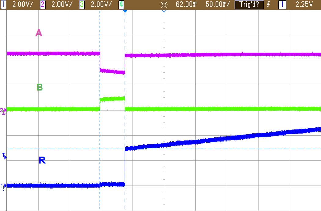 Figure 2-8 THVD1505 Powered Up with
Mis-wiring and Driver On
Figure 2-8 THVD1505 Powered Up with
Mis-wiring and Driver OnAs it is mentioned above, the bus voltage could be any value between 0-V and Vcc depending on the drive strength of the drivers at the two ends. In the test of SN65HVD888, the worst-case scenario happens – two drivers have similar drive capability and SN65HVD888 is stronger (Figure 2-9). The negative differential bus voltage does not force the SN65HVD888 to change its polarity. Therefore, the fight between two devices will never end: both drivers keep driving the bus in opposite polarities, the bus is locked, and system is stuck. Thus, the polarity-free device can never correct itself due to the wrong bus information.
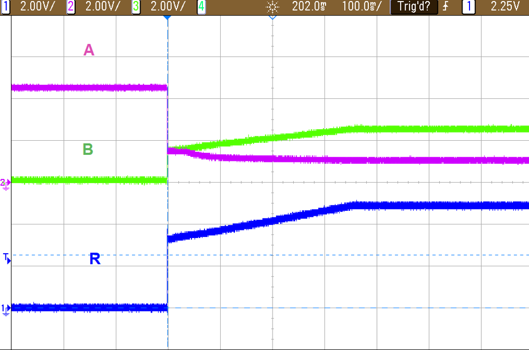 Figure 2-9 SN65HVD888 Powered Up with
Mis-wiring and Driver On