SLLA498 October   2020


  1.   1
  2.   2
  3.   3
    1.     4
    2.     5
  4.   6
    1.     7
    2.     8
    3.     9
  5.   10
    1.     11
    2.     12
    3.     13
    4.     14
    5.     15
    6.     16
    7.     17
  6.   18
    1.     19
    2.     20
    3.     21
    4.     22
    5.     23
    6.     24
  7.   25
    1.     26
    2.     27
  8.   28
  9.   29

Three-level TNPC Inverter

Figure 5-3 shows the basic topology of the three level T-Type Neutral Point Clamped (TNPC) inverter is depicted in . The TNPC inverter is an extension of the HERIC topology to suit three phase output. For 800-V DC link voltages, the high side and the low-side switch on each phase would usually be implemented with 1200-V IGBTs/MOSFETs as the full voltage has to be blocked by them. However, the bidirectional switches to the dc-link midpoint need to block only half of the voltage. It can be implemented with devices having a lower voltage rating like two 600-V IGBTs including anti-parallel diodes. Due to the reduced blocking voltage, the middle switch shows very low switching losses and acceptable conduction loss. If bipolar devices are used for the single 1200-V device, we can get reduced conduction losses, as the forward voltage drop of only one device occurs. This is in contrast to the NPC topology in which always two devices are conducting in series. The reduced conduction loss makes the TNPC an interesting choice even for low switching frequencies. As it is a three level topology, it has a good THD performance; and hence the inductor at the output can be smaller.
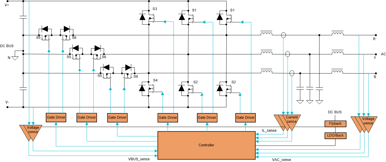
GUID-20200911-CA0I-XP6G-ZBDW-V5KL8WQG4N7S-low.gifFigure 5-3 Three-level TNPC Inverter.
While the conduction losses are significantly lower when compared with NPC, the switching losses are high due to the devices blocking full dc link voltage. Due to limited component count and better conduction losses compared to NPC topology, the TNPC topology is best suited for applications up to 40-kHz switching frequency; beyond which the NPC topology performs better. One of the drawbacks of this topology is the high peak voltage stress across the high voltage blocking FETs. The TI reference design 10kW 3-phase 3-level T-type inverter reference design for solar string inverter demonstrates the implementation of an inverter and the TI reference design Three-level, three-phase SiC AC-to-DC converter reference design demonstrates the implementation of a PFC stage of this type of power stage. This DC/AC topology being bidirectional, is an option to consider for the bidirectional DC/AC stage (see Figure 3-1) between the HV DC Bus and the AC Bus in a storage ready solar inverters.