• Menu
  • Product
  • Email
  • PDF
  • Order now
  • Manufacturing and Rework Design Guide for MicroSiP Power Modules

    • SLIB006A February   2011  – June 2021 TPS81256 , TPS82084 , TPS82085 , TPS82130 , TPS82140 , TPS82150 , TPS82670 , TPS82671 , TPS826711 , TPS826716 , TPS82672 , TPS826721 , TPS82673 , TPS82674 , TPS826745 , TPS82675 , TPS82676 , TPS826765 , TPS82677 , TPS8268090 , TPS8268105 , TPS8268120 , TPS8268150 , TPS8268180 , TPS82692 , TPS82693 , TPS82695 , TPS826951 , TPS82697 , TPS82698 , TPS82740A , TPS82740B , TPSM82810 , TPSM82813 , TPSM82816 , TPSM82821 , TPSM82821A , TPSM82822 , TPSM82822A , TPSM82823 , TPSM82823A


  • CONTENTS
  • SEARCH
  • Manufacturing and Rework Design Guide for MicroSiP Power Modules
  1. 1Introduction
  2. 2 MicroSiP Package
  3. 3PCB Layout
    1. 3.1 MicroSiP With BGA Pins
    2. 3.2 MicroSiL With LGA Pins
  4. 4Surface Mount Assembly
  5. 5Rework Guidelines
  6. 6FAQs
  7. 7Trademarks
  8. IMPORTANT NOTICE
search No matches found.
  • Full reading width
    • Full reading width
    • Comfortable reading width
    • Expanded reading width
  • Card for each section
  • Card with all content


USER'S GUIDE

Manufacturing and Rework Design Guide for MicroSiP Power Modules

1 Introduction

As the marketplace continues to demand size reductions in electronic products, the need for smaller packaging and smaller subsystem packaging becomes paramount. To address these rapidly evolving customer requirements, TI has developed MicroSiP™ power modules, an innovation in System-in-Package (SiP) technology to integrate both the IC and passive components into a single device.

With this technology, TI reaches the smallest solution size and highest levels of integration. This enables an easy-to-use power module for achieving the shortest time-to-market. As with any device package, attention must be given to the printed circuit board (PCB) layout, surface mount (SMT) assembly flow, and rework process. This white paper provides guidelines on each of these aspects, and these guidelines are achievable through normal manufacturing and rework flows.

2 MicroSiP Package

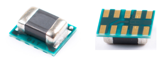
Within the MicroSiP family, there are two variations: MicroSiP (µSiP) and MicroSiL (µSiL). MicroSiP devices contain both the power inductor and one or more capacitors and typically use ball grid array (BGA) pins. MicroSiL devices contain just the power inductor and typically use land grid array (LGA) pins. The pin type difference creates different land pattern recommendations, but the SMT and rework guidelines remain the same for both packages. Figure 2-1 shows a typical MicroSiP with BGA pins, while Figure 2-2 shows a typical MicroSiL with LGA pins.


GUID-20210323-CA0I-WXVW-0LWD-HPCRKP5HRCNK-low.png

Figure 2-1 MicroSiP™ Package Integrates the Power Inductor and Two Capacitors and Uses BGA Pins
GUID-20210322-CA0I-XF4P-4NWL-HLKQXPDZ48H8-low.png

Figure 2-2 MicroSiL Package Integrates the Power Inductor and Uses LGA Pins

3 PCB Layout

3.1 MicroSiP With BGA Pins

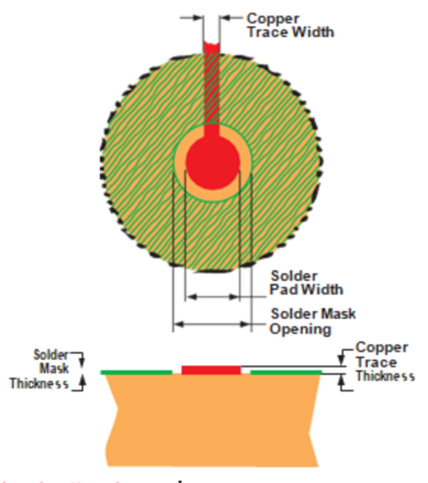
When designing the pads for MicroSiP devices with BGA pins, it is recommended that the layout use a non-solder mask defined (NSMD) pad. With this method, the solder mask opening is made larger than the desired land area, and the resulting copper size is defined solely by the size of the land pad of the device. Table 3-1 shows the appropriate pad design for MicroSiP™ devices with BGA pins. Specific recommendations are listed here and shown in Figure 3-1:

  • Circuit traces from the NSMD PCB pads should be 75-µm to 100-µm wide in the exposed area inside the solder mask opening. Wider trace widths reduce device standoff, which worsens board level reliability (BLR).
  • Best BLR results are achieved when the PCB laminate glass transition temperature is above the operating range of the application
  • Recommended solder paste is Type 3 or Type 4
  • For a PCB using a Ni/Au surface finish, the gold thickness should be less than 0.5 µm to avoid a reduction in thermal fatigue performance
  • Solder mask thickness should be less than 20 µm on top of the copper circuit pattern, to increase device standoff and improve BLR
  • Best solder stencil performance is achieved using laser cut stencils with electro-polishing. Use of chemically etched stencils gives inferior solder paste volume control.
Table 3-1 Recommended Pad Design for MicroSiP™ Devices With BGA Pins
Land Pattern Dimensions
Solder Pad TypeLand Pad WidthSolder Mask OpeningCopper ThicknessStencil OpeningStencil Thickness
Non-solder mask defined (NSMD)0.30 mm0.360 mm

1 oz max

(0.032 mm)

0.34 mm diameter0.1 mm

GUID-20210323-CA0I-X04M-G3MF-MBMLV9PQHLJG-low.png

Figure 3-1 Recommended Pad Design for MicroSiP™ Devices With BGA Pins

See the device data sheet for specific recommendations.

3.2 MicroSiL With LGA Pins

When designing the pads for the MicroSiL devices with LGA pins, SMD pads are usually recommended over NSMD pads. With a power module, some pins (such as VIN, VOUT, and GND) are typically connected to large copper planes to carry the current and heat away from the device. Such copper planes grow the pad size of a NSMD pad, which then thins the solder paste thickness. Using SMD pads keeps each pad the same size and avoids solder pulling the device during reflow. See the device data sheet for specific recommendations.

4 Surface Mount Assembly

Surface mounting of MicroSiP BGA and LGA packages is broadly similar to BGA and QFN package assembly, respectively. TI recommends the use of lead-free solder paste applied via a 0.1-mm thick stencil. The paste acts to aid wetting of the MicroSiP pin to the board land pad, to hold the device in place during reflow, and to contribute metal volume of the resultant solder joint. For the setup of a reflow profile, the JEDEC reflow profiles for near-eutectic SnAgCu solder alloys can be used as a starting point with soldering temperatures up to 250°C. The resulting solder joint height is typically around 120 µm. Figure 4-1 shows a cross-section of solder joints which attach three BGA pins to a four-layer PCB.


GUID-20210323-CA0I-KKV9-1913-QMZNRDVK7T7N-low.png

Figure 4-1 Cross-Section of a MicroSiP™ With BGA Pins on Top of a Four-Layer PCB

All MicroSiP devices passed BLR testing during their development. As an example, 8-pin MicroSiP devices with BGA pins were assembled after preconditioning with no underfill or adhesive used. Table 4-1 shows the BLR test results.

Table 4-1 Board-Level Reliability Testing for 8-Pin MicroSiP™ Devices With BGA Pins
Test Parameters Results (tfirst fail)
Drop 1500 G, 1.0 ms pulse > 100 drops
Temperature Cycle –40, 125°C, 2 cycles/hr > 1000 cycles

The surface mounting process of MicroSiP devices with LGA pins is similar to a QFN package assembly. Irregular surface plating, uneven solder paste thickness, and crowning of the solder plating can reduce overall surface mounting yields. Bare copper with an organic solderability preservative (OSP) coating, tin (Sn) plating or electro-less nickel immersion gold (ENIG) have been shown to provide an acceptable land pad surface.

The advantages of plating over OSPs are better shelf life, permanent coverage of copper vias and other features not exposed to a solder process, and contamination resistance. Even with these differences, OSPs have shown robust performance in the industry. In summary, a controlled assembly process for soldering MicroSiP devices with LGA pins package relies on a flat, uniform PCB pad surface. Achieving a flat, uniform surface leads to a greater control of solder paste uniformity, resulting in an overall robust process. See the QFN and SON PCB Attachment application report for more details on soldering QFN packages.

As explained in the QFN and SON PCB Attachment application report, all devices (including MicroSiPs) need to be placed carefully to avoid regions of extreme deflection, if the PCB will be subject to excessive bending during manufacturing. Excessive bending of the PCB can lead to package damage and should be avoided in the assembly flow.


GUID-20210323-CA0I-6H0Q-WKDP-XRQ337JBSLZ4-low.png

Figure 4-2 Avoid Excessive Bending

5 Rework Guidelines

TI strongly recommends that the PCB with already-mounted SMT devices be baked prior to any rework so that absorbed moisture is removed. See J-STD-033 for more details. The rework process should be characterized such that the temperature of the MicroSiP device and the surrounding PCB area are controlled. Either an attached thermocouple or an infrared camera works well to determine a repeatable heating profile.

Component removal process example:

  • Align nozzle over part to be removed
  • Maintain nozzle 1.27 mm over the package
  • Preheat board to 90°C, nozzle warming at 20% airflow, 125°C
  • Soak stage at 20% air flow, 225°C, 90 seconds
  • Ramp stage at 25% air flow, 335°C, 30 seconds
  • Reflow stage at 25% air flow, 370°C, 65 seconds
  • Enable vacuum, lower nozzle, remove inductor and capacitors from MicroSiP
  • Discard inductor and capacitors
  • Reposition nozzle, reheat at 25% air flow, 370°C, 20 seconds
  • Enable vacuum, lower nozzle, remove MicroSiP from PCB
  • Cool down stage at 40% air flow, 25°C, 50 seconds
  • Turn off vacuum and remove MicroSiP from nozzle
  • Avoid handling damage of the removed unit
  • Do not reuse or repair the removed unit

Component replacement process example:

  • Apply solder paste to board using a micro-stencil
  • Align MicroSiP over board land pads
  • Place MicroSiP on board. Care should be taken to prevent overtravel during placement which may damage the package or vacuum tip
  • Raise nozzle 1.27 mm
  • Preheat board to 90°C, nozzle warming at 20% air flow, 125°C
  • Soak stage at 20% air flow, 225°C, 90 seconds
  • Ramp stage at 25% air flow, 335°C, 30 seconds
  • Reflow stage at 25% air flow, 370°C, 65 seconds
  • Cool down stage at 40% air flow, 25°C, 50 seconds

Air-Vac Engineering:

Air-Vac Engineering (www.air-vac-eng.com) has established heating profiles and tooling recommendations for their Hot Gas (convection) rework equipment, DRS-24NC.

Nozzle NMX188DVG:

  • 0.18 in exhaust opening
  • VTMX020-35 vacuum tip

Comparable hot gas (convection heating) rework equipment from other vendors can also be used successfully.

6 FAQs

Q: What is a MicroSiP™?

A: MicroSiP™ is a miniaturized System-in-Package (SiP) that integrates silicon integrated circuits (ICs) with passive components in a BGA or LGA footprint format.

Q: Is this a lead-free (Pb-free) package?

A: Yes. MicroSiP packages comply with lead-free environmental policies and are RoHS compliant. The BGA bumps and the solder joints on the inductor and capacitors use SAC305 solder paste (3% Ag, 0.5% Cu, 96.5% Sn). Devices with LGA pins have either a NiAu finish (from the electroless nickel immersion gold (ENIG) process) or have a NiPdAu finish (from the electroless nickel electroless palladium immersion gold (ENEPIG) process). The related product folder states which lead finish a particular device has.

Q: Are there any special MicroSiP™ placement requirements?

A: Movement of the MicroSiP from the tape and reel (T&R) to placement on the PCB can be treated as a similar sized BGA or QFN. The nozzle should make contact with the MicroSiP device in the location noted in the package drawing in the data sheet. This is usually on the inductor. The recommended nozzle size is also stated in the package drawing in the data sheet. For MicroSiP devices with BGA pins, an approximate 1-mm diameter nozzle/rubber tip is recommended with a contact area between 0.5–1.0 mm2.

Q: Can I mount MicroSiP to the bottom of the PCB board?

A: Yes. Ideally, the first and second reflow profiles are identical. The reflow profile should follow JEDEC standards for SMT of near-eutectic SnAgCu solder.

Q: Can the MicroSiP™ withstand multiple reflows?

A: Yes. The package is qualified for 3 reflow passes to accommodate first and second side board assembly and a nearby component repair cycle.

Q: What alignment accuracy is possible?

A: TI recommends printing a lead-free solder paste, as described in the PCB layout subsection, before placement of the MicroSiP. Alignment accuracy depends on the pad tolerance of the board and the MicroSiP placement accuracy. MicroSiP packages self-align during reflow—final alignment accuracy is very likely better than the placement accuracy.

Q: Are the integrated inductors shielded?

A: The chip inductor technology used in MicroSiP power modules entirely encloses the inductor winding for maximum shielding. Most MicroSiP devices use an inductor with a magnetic mold compound for best shielding.

Q: How can I measure the temperature of a MicroSiP module?

A: Each MicroSiP data sheet provides safe operating area (SOA) curves that show the thermal limits of the power module on the evaluation module (EVM). If the actual surface temperature of the MicroSiP is desired, a fiber optic temperature measurement setup yields the most accurate results. Many infrared (IR) imaging cameras display lower temperatures than in reality due to reflections off of the integrated inductor on the MicroSiP. Using a thin NiCrNi Thermal couple attached to the integrated inductor can be another precise method to measure the inductor temperature. Use the method described in the application report, An Accurate Thermal-Evaluation Method for the TLV62065 to measure the internal die temperature.

Q: Do I need to solder the exposed thermal pad on the bottom of the MicroSiP?

A: Yes. Just like for most discrete ICs and QFN-packaged devices, the exposed thermal pad (if present) must be soldered to the PCB. It is also recommended to place thermal vias under the exposed thermal pad for maximum height transfer, since the exposed thermal pad is the primary path of heat removal for many MicroSiPs.

Q: How does TI maintain supply chain continuity with the multiple components in each MicroSiP?

A: The passive components used in MicroSiPs are almost always catalog, off-the-shelf components available at multiple suppliers. See also TI’s Product Longevity Statement.

Q: Are MicroSiP modules compliant with EMI standards?

A: Many MicroSiPs, such as the TPSM82823, TPS82085 and LMZ20502, are compliant with CISPR standards for radiated emissions. Consult the device data sheet to see if a specific module has been tested.

Q: What is the difference between solder mask defined (SMD) and non-solder mask defined (NSMD) land pads?

A: In an SMD pad, there is a flood of copper and the solder mask is pulled back to expose the land pad. There is copper in the entire solder mask opening and extending under the solder mask. In a NSMD pad, the solder mask is pulled back to expose both the copper land pad and a gap between the copper land pad and the solder mask. Since many pins of a MicroSiP are routed to copper pours and planes, the NSMD gap between the copper and the solder mask is filled with copper and the land pad size is larger than expected. SMD land pads usually provide a more consistent land pad size for MicroSiLs with LGA pins, which results in improved solderability. Consult the specific device data sheet and its package drawing for the recommended land pattern. Figure 6-1 shows the difference in SMD and NSMD pads.


GUID-20210323-CA0I-CBWZ-JKWM-FF6JBPMWZ3TC-low.png

Figure 6-1 NSMD Pads Create a Gap Between the Exposed Copper and the Solder Mask, While SMD Pads Expose Only Copper Without any Gap

7 Trademarks

MicroSiP are trademarks of Texas Instruments Incorporated.

All trademarks are the property of their respective owners.

IMPORTANT NOTICE AND DISCLAIMER

TI PROVIDES TECHNICAL AND RELIABILITY DATA (INCLUDING DATASHEETS), DESIGN RESOURCES (INCLUDING REFERENCE DESIGNS), APPLICATION OR OTHER DESIGN ADVICE, WEB TOOLS, SAFETY INFORMATION, AND OTHER RESOURCES “AS IS” AND WITH ALL FAULTS, AND DISCLAIMS ALL WARRANTIES, EXPRESS AND IMPLIED, INCLUDING WITHOUT LIMITATION ANY IMPLIED WARRANTIES OF MERCHANTABILITY, FITNESS FOR A PARTICULAR PURPOSE OR NON-INFRINGEMENT OF THIRD PARTY INTELLECTUAL PROPERTY RIGHTS.
These resources are intended for skilled developers designing with TI products. You are solely responsible for (1) selecting the appropriate TI products for your application, (2) designing, validating and testing your application, and (3) ensuring your application meets applicable standards, and any other safety, security, or other requirements. These resources are subject to change without notice. TI grants you permission to use these resources only for development of an application that uses the TI products described in the resource. Other reproduction and display of these resources is prohibited. No license is granted to any other TI intellectual property right or to any third party intellectual property right. TI disclaims responsibility for, and you will fully indemnify TI and its representatives against, any claims, damages, costs, losses, and liabilities arising out of your use of these resources.
TI’s products are provided subject to TI’s Terms of Sale (www.ti.com/legal/termsofsale.html) or other applicable terms available either on ti.com or provided in conjunction with such TI products. TI’s provision of these resources does not expand or otherwise alter TI’s applicable warranties or warranty disclaimers for TI products.
Mailing Address: Texas Instruments, Post Office Box 655303, Dallas, Texas 75265
Copyright © 2020, Texas Instruments Incorporated


Texas Instruments

© Copyright 1995-2025 Texas Instruments Incorporated. All rights reserved.
Submit documentation feedback | IMPORTANT NOTICE | Trademarks | Privacy policy | Cookie policy | Terms of use | Terms of sale