SFFS451 September 2022 TPS7B69-Q1
4.2 SOT-23 Package
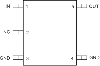
Figure 4-2 shows the TPS7B69-Q1 pin diagram for the SOT-23 package. For a detailed description of the device pins, see the Pin Configuration and Functions section in the TPS7B69-Q1 data sheet.
 Figure 4-2 Pin Diagram (SOT-23 Package)
Table 4-6 Pin FMA for Device Pins
Short-Circuited to Ground
| Pin Name | Pin No. | Description of Potential Failure Effects | Failure Effect Class |
|---|---|---|---|
| IN | 1 | No output voltage. System performance depends on the upstream current limit. | B |
| NC | 2 | No effect. Normal operation. | D |
| GND | 3 | No effect. Normal operation. | D |
| GND | 4 | No effect. Normal operation. | D |
| OUT | 5 | Current limit is triggered, and the device can repeatedly enter and exit thermal shutdown depending on power dissipation. | B |
Table 4-7 Pin FMA for Device Pins
Open-Circuited
| Pin Name | Pin No. | Description of Potential Failure Effects | Failure Effect Class |
|---|---|---|---|
| IN | 1 | Power is not supplied to the device, resulting in no output voltage. | B |
| NC | 2 | No effect. Normal operation. | D |
| GND | 3 | A floating GND pin can result in incorrect voltage regulation or no output voltage. | B |
| GND | 4 | A floating GND pin can result in incorrect voltage regulation or no output voltage. | B |
| OUT | 5 | The output is disconnected from the load. | B |
Table 4-8 Pin FMA for Device Pins
Short-Circuited to Adjacent Pin
| Pin Name | Pin No. | Shorted to | Description of Potential Failure Effects | Failure Effect Class |
|---|---|---|---|---|
| IN | 1 | NC | No effect. Normal operation. | D |
| NC | 2 | GND | No effect. Normal operation. | D |
| GND | 3 | GND | No effect. Normal operation. | D |
| GND | 4 | OUT | Current limit is triggered, and the device can repeatedly enter and exit thermal shutdown depending on power dissipation. | B |
Table 4-9 Pin FMA for Device Pins
Short-Circuited to
supply
| Pin Name | Pin No. | Description of Potential Failure Effects | Failure Effect Class |
|---|---|---|---|
| IN | 1 | No effect. Normal operation. | D |
| NC | 2 | No effect. Normal operation. | D |
| GND | 3 | No output voltage. System performance depends on the upstream current limit. | B |
| GND | 4 | No output voltage. System performance depends on the upstream current limit. | B |
| OUT | 5 | The output is not regulated. VOUT = VIN. The OUT pin can be damaged if the absolute maximum rating (7 V) is violated. | B/A |