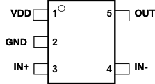
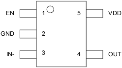
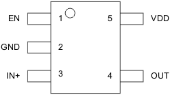
This section provides a Failure Mode Analysis (FMA) for the pins of the UCC27517A-Q1. The failure modes covered in this document
include the typical pin-by-pin failure scenarios:
Table 4-2 through Table 4-8 also indicate how these pin conditions can affect the device as per the failure
effects classification in Table 4-1.
Table 4-1 TI Classification of Failure Effects| Class | Failure Effects |
|---|
| A | Potential device damage that affects
functionality |
| B | No device damage, but loss of functionality |
| C | No device damage, but performance degradation |
| D | No device damage, no impact to functionality or
performance |
Figure 4-1 shows the UCC27517A-Q1
UCC27518A-Q1
UCC27519A-Q1 pin diagram. For a detailed description of
the device pins please refer to the Pin Configuration and Functions section
in the data sheet.
Following are the assumptions of use and the device configuration assumed for the pin
FMA in this
section:
- Pin #4 and 5 short case not considered.
- Short between corner pins are not
considered.
Table 4-2 Pin FMA for Device Pins
Short-Circuited to Ground
| Pin Name |
Pin No. |
UCC27517A-Q1 Description of Potential
Failure Effect(s) |
Failure Effect Class |
| VDD |
1 |
VDD and GND short circuit. No power is
applied to the device. |
D |
| GND |
2 |
Short to same potential. No
impact. |
D |
| IN+ |
3 |
OUT stuck low. |
B |
| IN- |
4 |
OUT responds to IN+. IN- stuck low. |
B |
| OUT |
5 |
Posiible OUT pin and driver
damge. |
A |
Table 4-3 Pin FMA for Device Pins Short-Circuited to Ground
| Pin Name |
Pin No. |
UCC27518A-Q1
UCC27519A-Q1Description of Potential
Failure Effect(s) |
Failure Effect Class |
| EN |
1 |
OUT is disabled |
B |
| GND |
2 |
Short to same potential. No
impact. |
D |
| IN- |
3 |
OUT stuck high. |
B |
| IN+ |
3 |
OUT stuck low |
B |
| OUT |
4 |
Posiible OUT pin and driver
damge. |
A |
| VDD |
5 |
VDD and GND short circuit. No power is
applied to the device. |
D |
Table 4-4 Pin FMA for Device Pins
Open-Circuited
| Pin Name |
Pin No. |
Description of Potential Failure Effect(s) |
Failure Effect Class |
| VDD |
1 |
No power is applied to the
device. |
D |
| GND |
2 |
OUT is pulled up to VDD level. |
B |
| IN+ |
3 |
OUT stuck low. |
B |
| IN- |
4 |
OUT stuck low. |
B |
| OUT |
5 |
OUT operates normally. Connection to
the gate of Power FET is lost. |
B |
Table 4-5 Pin FMA for Device Pins Open-Circuited
| Pin Name |
Pin No. |
UCC27518A-Q1
UCC27519A-Q1Description of Potential
Failure Effect(s) |
Failure Effect Class |
| EN |
1 |
OUT is enabled |
B |
| GND |
2 |
OUT stuck high. |
B |
| IN- |
3 |
OUT stuck low. |
B |
| IN+ |
3 |
OUT stuck low. |
B |
| OUT |
4 |
OUT is floating |
B |
| VDD |
5 |
No power is applied to the
device. |
B |
Table 4-6 Pin FMA for Device Pins
Short-Circuited to Adjacent Pin
| Pin Name |
Pin No. |
Shorted to |
Description of Potential Failure Effect(s) |
Failure Effect Class |
| VDD |
1 |
GND |
VDD and GND short circuit. No power is
applied to the device. |
D |
| GND |
2 |
IN+ |
OUT stuck low. |
B |
Table 4-7 Pin FMA for Device Pins Short-Circuited to Adjacent Pin
| Pin Name |
Pin No. |
Shorted to |
UCC27518A-Q1
UCC27519A-Q1 Description of Potential
Failure Effect(s) |
Failure Effect Class |
| EN |
1 |
GND |
OUT is disabled |
B |
| GND |
2 |
IN- |
OUT stuck high. |
B |
| GND |
2 |
IN+ |
OUT stuck low. |
B |
Table 4-8 Pin FMA for Device Pins
Short-Circuited to
supply
| Pin Name |
Pin No. |
Description of Potential Failure Effect(s) |
Failure Effect Class |
| VDD |
1 |
Short to same potential. No
impact. |
D |
| GND |
2 |
VDD and GND short circuit. No power is
applied to the device. |
D |
| IN+ |
3 |
OUT stuck high if IN- is low. |
B |
| IN- |
4 |
OUT stuck low. |
B |
| OUT |
5 |
Possible OUT pin and driver
damge. |
A |
Table 4-9 Pin FMA for Device Pins Short-Circuited to supply
| Pin Name |
Pin No. |
UCC27518A-Q1
UCC27519A-Q1Description of Potential
Failure Effect(s) |
Failure Effect Class |
| EN |
1 |
OUT is enabled. EN is stuck
high. |
B |
| GND |
2 |
VDD and GND short circuit. No power is
applied to the device. |
D |
| IN- |
3 |
OUT stuck low. |
B |
| IN+ |
3 |
OUT stuck high. |
B |
| OUT |
4 |
Possible OUT pin and driver
damge. |
A |
| VDD |
5 |
Short to same potential. No
impact. |
D |
 Figure 4-1 UCC27517A-Q1 Pin Diagram
 Figure 4-2 UCC27518A-Q1 Pin Diagram
 Figure 4-3 UCC27519A-Q1