SFFS048 January 2021 DRV8872-Q1
4 Pin Failure Mode Analysis (Pin FMA)
This section provides a Failure Mode Analysis (FMA) for the pins of the DRV8872-Q1. The failure modes covered in this document include the typical pin-by-pin failure scenarios:
- Pin short-circuited to Ground (see Table 4-2)
- Pin open-circuited (see Table 4-3)
- Pin short-circuited to an adjacent pin (see Table 4-4)
- Pin short-circuited to supply (see Table 4-5)
Table 4-2 through Table 4-5 also indicate how these pin conditions can affect the device as per the failure effects classification in Table 4-1.
| Class | Failure Effects |
|---|---|
| A | Potential device damage that affects functionality |
| B | No device damage, but loss of functionality |
| C | No device damage, but performance degradation |
| D | No device damage, no impact to functionality or performance |
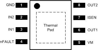
Figure 4-1 shows the DRV8872-Q1 pin diagram. For a detailed description of the device pins please refer to the Pin Configuration and Functions section in the DRV8872-Q1 data sheet.
 Figure 4-1 Pin Diagram
Following are the assumptions of use and the device configuration assumed for the pin FMA in this section:
- The device is used with external components consistent with the values described in the external component table of the datasheet.
| Pin Name | Pin No. | Description of Potential Failure Effect(s) | Failure Effect Class |
|---|---|---|---|
| GND | 1 | Intended operation | D |
| IN2 | 2 | OUTx driver control will be lost | B |
| IN1 | 3 | OUTx driver control will be lost | B |
| nFAULT | 4 | Device will always signal fault | B |
| VM | 5 | Device will not power up | B |
| OUT1 | 6 | OUTx HiZ, with device signaling fault | B |
| ISEN | 7 | Current regulation capability will be lost | B |
| OUT2 | 8 | OUTx HiZ, with device signaling fault | B |
| Pin Name | Pin No. | Description of Potential Failure Effect(s) | Failure Effect Class |
|---|---|---|---|
| GND | 1 | Device will not power up | B |
| IN2 | 2 | OUTx driver control will be lost | B |
| IN1 | 3 | OUTx driver control will be lost | B |
| nFAULT | 4 | Fault signaling will be lost | B |
| VM | 5 | Device will not power up | B |
| OUT1 | 6 | OUT1 driver control will be lost | B |
| ISEN | 7 | OUT1 and OUT2 driver control will be lost | B |
| OUT2 | 8 | OUT2 driver control will be lost | B |
| Pin Name | Pin No. | Shorted to | Description of Potential Failure Effect(s) | Failure Effect Class |
|---|---|---|---|---|
| GND | 1 | IN2 | OUTx driver control will be lost | B |
| IN2 | 2 | IN1 | OUTx driver control will be lost | B |
| IN1 | 3 | nFAULT | OUTx driver control will be lost, fault signaling will be lost | B |
| nFAULT | 4 | VM | Low voltage pin max voltage violated | A |
| VM | 5 | OUT1 | OUTx HiZ, with device signaling fault | B |
| OUT1 | 6 | ISEN | Low voltage pin max voltage violated | A |
| ISEN | 7 | OUT2 | Low voltage pin max voltage violated | A |
| OUT2 | 8 | GND | OUTx HiZ, with device signaling fault | B |
| Pin Name | Pin No. | Description of Potential Failure Effect(s) | Failure Effect Class |
|---|---|---|---|
| GND | 1 | Device will not power up | B |
| IN2 | 2 | Low voltage pin max voltage violated | A |
| IN1 | 3 | Low voltage pin max voltage violated | A |
| nFAULT | 4 | Low voltage pin max voltage violated | A |
| VM | 5 | Intended operation | D |
| OUT1 | 6 | OUTx HiZ, with device signaling fault | B |
| ISEN | 7 | Low voltage pin max voltage violated | A |
| OUT2 | 8 | OUTx HiZ, with device signaling fault | B |