SBVA093 December 2022 LP2992 , TPS786 , TPS7A30 , TPS7A3001-EP , TPS7A33 , TPS7A39 , TPS7A4501-SP , TPS7A47 , TPS7A47-Q1 , TPS7A4701-EP , TPS7A49 , TPS7A52 , TPS7A52-Q1 , TPS7A53 , TPS7A53-Q1 , TPS7A53A-Q1 , TPS7A53B , TPS7A54 , TPS7A54-Q1 , TPS7A57 , TPS7A7100 , TPS7A7200 , TPS7A7300 , TPS7A80 , TPS7A8300 , TPS7A83A , TPS7A84 , TPS7A84A , TPS7A85 , TPS7A85A , TPS7A87 , TPS7A89 , TPS7A90 , TPS7A91 , TPS7A92 , TPS7A94 , TPS7A96 , TPS7B7702-Q1 , TPS7H1111-SEP , TPS7H1111-SP , TPS7H1210-SEP
5 Impacts and Opportunities of PCB Parasitic Impedance
PCB parasitic impedance increases the effective ballast resistance. In designs with a large value discrete ballast resistor (such as greater than 50 mΩ), Equation 10 and Equation 6 provides good approximations of the load current and voltage. For small values of ballast resistance (such as less than 50 mΩ), the parasitic PCB impedance can impact the final current sharing analysis. To enable high performance use cases, RB can be optimized by reviewing the PCB parasitic impedance and reducing the discrete ballast resistance for each LDO accordingly. A reduction of RB will increase the current sharing mismatch between each LDO Equation 10 but will increase the load voltage Equation 6 which is usually a desired result.
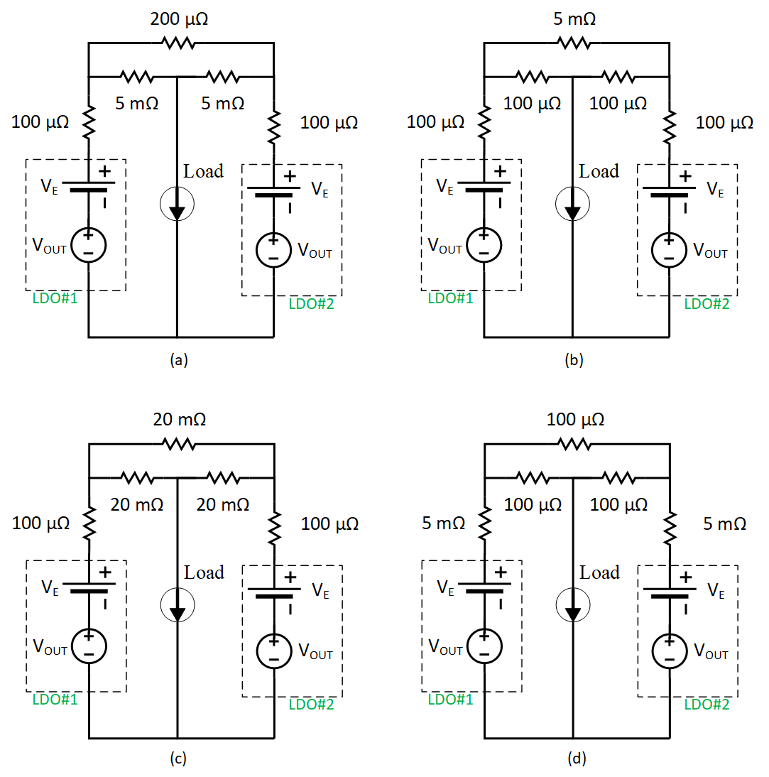
The interaction of the ballast resistance and PCB impedance is shown in Figure 5-1 assuming a minimum 5 mΩ ballast is needed. Here, we will limit the discussion to two parallel LDO's although we can extend this to any number of parallel LDO's. The PCB impedance is lumped into one equivalent resistor from each LDO to the load and also between the LDOs. Figure 5-1 then provides the four possible use cases of discrete ballast resistance and PCB impedance. Figure 5-1 (a) and Figure 5-1 (b) show insufficient ballast resistance between the LDOs or between the LDO and the load, which is incorrect and could lead to a current fault condition. Figure 5-1 (c) will current share but the load voltage specification may not be met due to the larger 20 m-ohm impedances. Figure 5-1 (d) is an example where the ballast resistance and PCB impedance has been optimized.
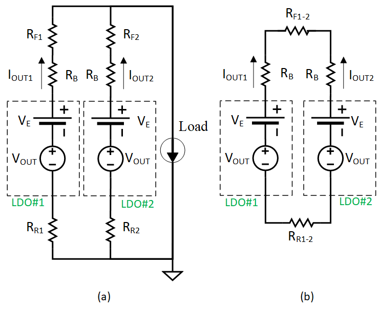
Thus, from Figure 5-1 (a) and (b) there are two sets of PCB impedance which must be reviewed in a system and are illustrated in Figure 5-2 for two parallel LDO's. From Figure 5-2a, RF1 and RF2 are the parasitic impedances from the output of each ballast resistor to the load, while RR1 and RR2 is the parasitic impedance from the load to the return pin of each LDO. From Figure 5-2b, RF1-2 is the parasitic impedance between the output side of the ballast resistors used for LDOs 1 and 2 and RR1-2 is the parasitic impedance between the LDO 1 and 2 return pins. Note that RF1-2≠ RF1 + RF2 and RR1-2≠ RR1 + RR2.

| (a) The LDO outputs are connected before the ballast resistor (b) The load is connected before the ballast resistors. (c) The LDO's will current share but the load regulation may not meet the requirements. (d) Optimum configuration of ballast resistance and PCB impedance. |

| (a) Equivalent circuit from each voltage regulator to the load. (b) Equivalent circuit from one voltage regulator to another voltage regulator. |
The parasitic impedances RF1, RF2, RR1, RR2, RF1-2, and RR1-2 can be simulated using a post route simulator, such as Altium PDN analysis. Note that when evaluating the parasitic return impedance, thermal pads should not be included in the post route simulation as the point of return for the simulated load. Thermal pads provide a low thermal resistance to dissipate heat, however they do not provide low electrical resistance from the die to ground. Thus, the simulation should be performed back to the ground pin of the LDO.
Upon review of Figure 5-2a, we wish to identify the minimum discrete ballast resistance RBn’ necessary to meet Equation 9 by accounting for RFn and RRn.
Upon review of Figure 5-2b, we wish to identify the minimum discrete ballast resistance RB’ necessary to meet Equation 9 while accounting for RF1-2 and RR1-2.
The new, optimized ballast resistor RB_OPT chosen to account for the parasitic PCB impedance is the maximum value of RBn’ and RB’ as shown in Equation 16. IOUTn and VLOAD can be modified as shown in Equation 17 and Equation 18, respectively. If both RBn’ and RB’ provide negative values, then the PCB impedance is higher than the necessary ballast resistance for the desired worst-case current sharing. Thus, a discrete ballast resistor can be removed from the design as the parasitic impedances provide sufficient ballast resistance.
If the voltage at the load must be increased, the PCB impedances can be reduced and / or VOUTn can be increased to achieve a higher VLOAD.