SBOA527 November 2021 INA901-SP
4 Summary
This application note demonstrates two separate topologies for bidirectional design of the INA901-SP, and provides executed bench tests to demonstrate that less than one percent error over a wide current operating range is potentially achievable via use of these topologies when a calibration is able to be performed.
Care must be taken when implementing such a system, as challenges and pitfalls do exist, as the method for this implementation is observed as an erroneous measurement when using the INA901, or any current sense amplifier for that matter, in its normal operating use case.
Finally, it is observed that for optimal results from the viewpoint of part count, propagation delay, or many other potential factors, the design must be compartmentalized into a specific use case such as high- or low-side sensing, and these use cases are unable to be deviated from. The following conclusions for the two circuits were made:
- In the case of low-side sensing, the VCM of the IN+ pin must be held to less than that of the supply voltage to ensure proper operation. While implementation on the high side may be possible, provided the condition 0 < VCM+VSENSE < VS is satisfied, this seems impractical, and this potential use case was not explored.
- In the case of high-side sensing, the VCM of the IN– pin must be held to less than that of the established REF voltage of the TL1431-SP, which is 2.5 V.
These conclusions show that neither design is common-mode independent, and the common mode of the design must be taken into account to ensure that invalid use cases will not be performed.
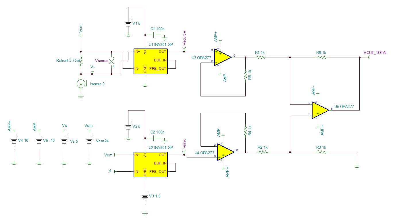
Due diligence was conducted on additional topologies that potentially operate independently of the amplifier VCM, but were ultimately shelved due to high part count, the need to operate within the < 20-mV sense condition, propagation delay of the circuitry, and complexity of design. Figure 4-1 and Figure 4-2 illustrate an example of one of these topologies, without comment, as a starting point for potential operating use cases that require this need, but it is left to the reader as to the potential fit for their given system. Due to the delays of the signal chain, such designs should only be used for applications such as telemetry, and not time-sensitive applications such as overcurrent protection or motor control. Note that even this circuit is slightly common-mode limited, due to the 1.5-V referenced GND of component U2.
 Figure 4-1 INA901 Bidirectional Design With
Independent VCM (–13.5 V to 65 V)
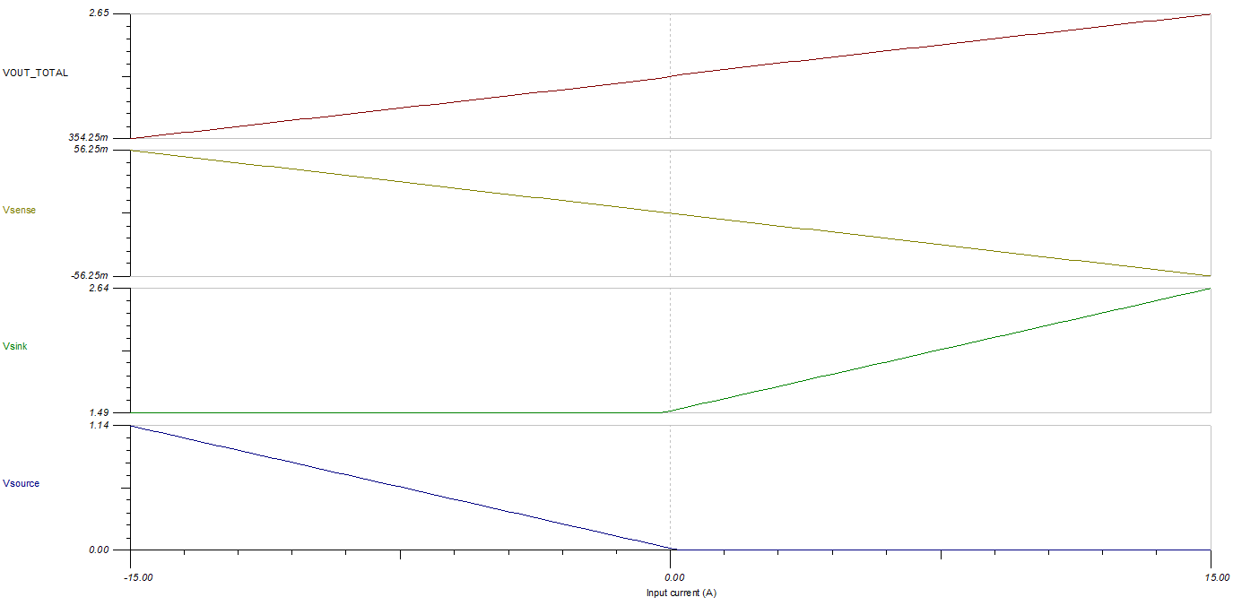
 Figure 4-2 INA901 Independent VCM Design
Simulated Results