ZHCSFJ6B August 2016 – March 2022 UCD9090A
PRODUCTION DATA
- 1 特性
- 2 应用
- 3 说明
- 4 Revision History
- 5 Pin Configuration and Functions
- 6 Specifications
-
7 Detailed Description
- 7.1 Overview
- 7.2 Functional Block Diagram
- 7.3 Feature Description
- 7.4
Device Functional Modes
- 7.4.1 Power Supply Sequencing
- 7.4.2 Pin-Selected Rail States
- 7.4.3 Monitoring
- 7.4.4 Fault Responses and Alert Processing
- 7.4.5 Shut Down All Rails and Sequence On (Resequence)
- 7.4.6 GPIOs
- 7.4.7 GPO Control
- 7.4.8 GPO Dependencies
- 7.4.9 GPI Special Functions
- 7.4.10 Power Supply Enables
- 7.4.11 Cascading Multiple Devices
- 7.4.12 PWM Outputs
- 7.4.13 Programmable Multiphase PWMs
- 7.4.14 Margining
- 7.4.15 Run Time Clock
- 7.4.16 System Reset Signal
- 7.4.17 Watch Dog Timer
- 7.4.18 Data and Error Logging to Flash Memory
- 7.4.19 Brownout Function
- 7.4.20 PMBus Address Selection
- 7.4.21 Device Reset
- 7.4.22 JTAG Interface
- 7.4.23 Internal Fault Management and Memory Error Correction (ECC)
- 7.5 Programming
- 8 Application and Implementation
- 9 Power Supply Recommendations
- 10Layout
- 11Device and Documentation Support
- 12Mechanical, Packaging, and Orderable Information
封装选项
请参考 PDF 数据表获取器件具体的封装图。
机械数据 (封装 | 引脚)
- RGZ|48
散热焊盘机械数据 (封装 | 引脚)
- RGZ|48
订购信息
7.3.3 Rail Configuration
A rail includes voltage, a power supply enable and a margining output. At least one must be included in a rail definition. Once the user has defined how the power supply rails should operate in a particular system, analog input pins and GPIOs can be selected to monitor and enable each supply (Figure 7-1).
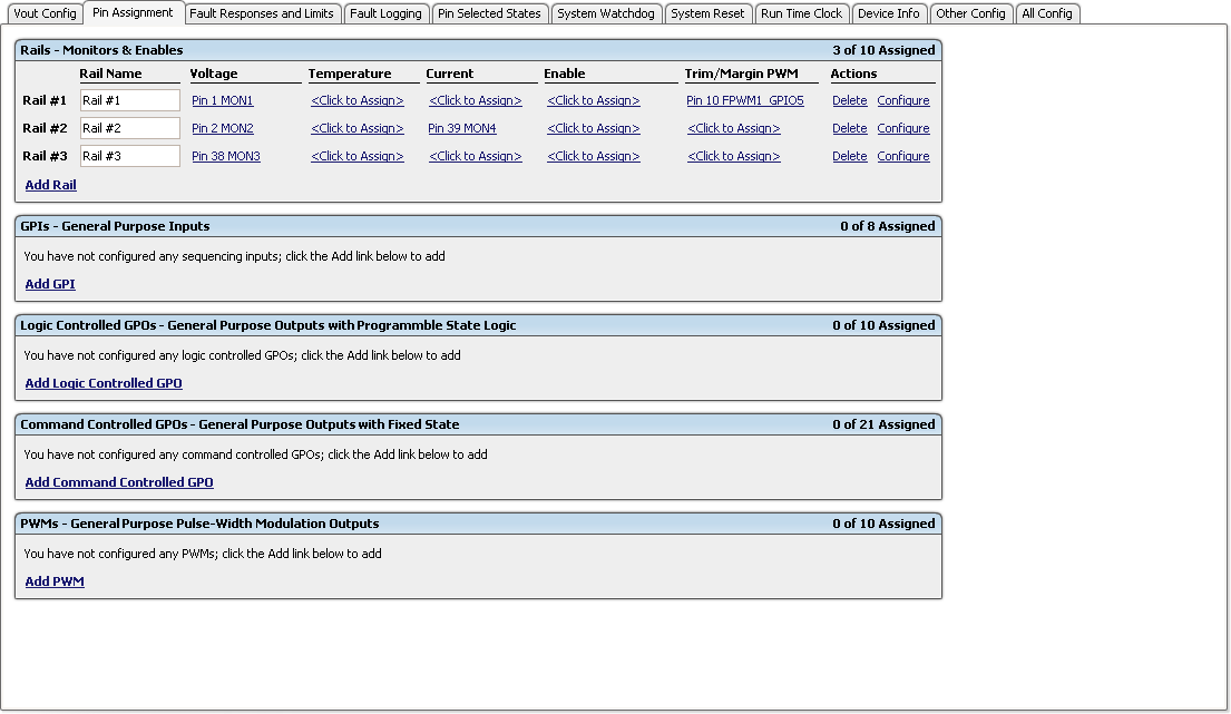 Figure 7-1 Fusion GUI Pin-Assignment Tab
After the pins have been configured, other key monitoring and sequencing criteria are selected for each rail from the VOUT Config tab (Figure 7-2):
- Nominal operating voltage (VOUT)
- Undervoltage (UV) and overvoltage (OV) warning and fault limits
- Margin-low and margin-high values
- Power-good on and power-good off limits
- PMBus or pin-based sequencing control (On/Off Config)
- Rails, GPOs, and GPIs for Sequence On dependencies
- Rails, GPOs, and GPIs for Sequence Off dependencies
- Turn-on and turn-off delay timing
- Maximum time allowed for a rail to reach POWER_GOOD_ON or POWER_GOOD_OFF after being enabled or disabled
- Other rails to turn off in case of a fault on a rail (fault-shutdown slaves)
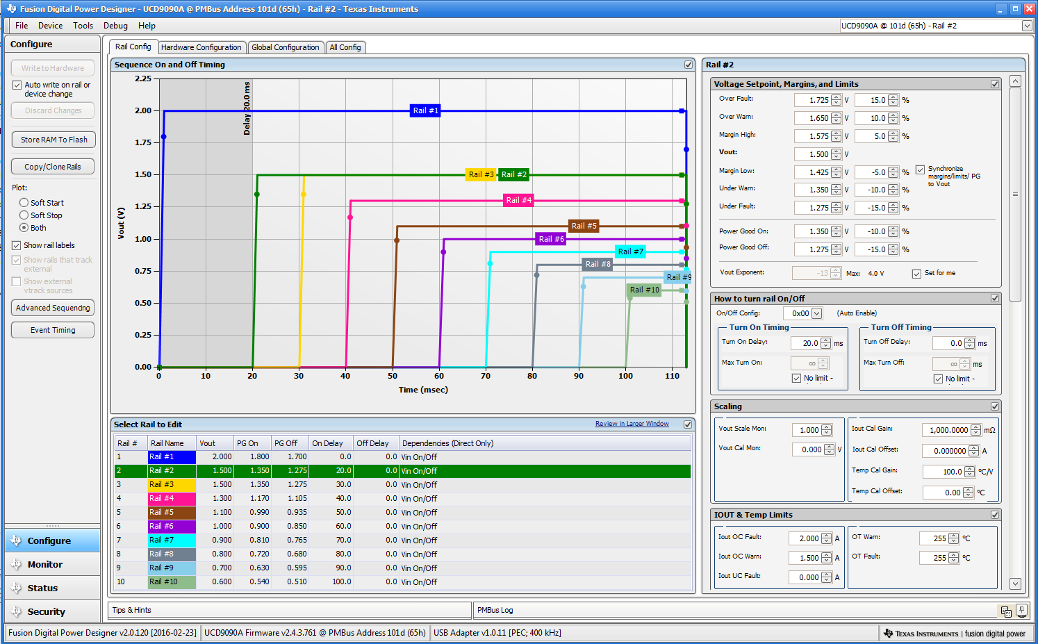 Figure 7-2 Fusion GUI VOUT-Config Tab
The Synchronize margins/limits/PG to Vout checkbox is an easy way to change the nominal operating voltage of a rail and also update all of the other limits associated with that rail according to the percentages shown to the right of each entry.
The plot in the upper left section of Figure 7-2 shows a simulation of the overall sequence-on and sequence-off configuration, including the nominal voltage, the turnon and turnoff delay times, the power-good on and power-good off voltages and any timing dependencies between the rails.
After a rail voltage has reached its POWER_GOOD_ON voltage and is considered to be in regulation, it is compared against two UV and two OV thresholds in order to determine if a warning or fault limit has been exceeded. If a fault is detected, the UCD9090A responds based on a variety of flexible, user-configured options. Faults can cause rails to restart, shut down immediately, sequence off using turnoff delay times or shut down a group of rails and sequence them back on. Different types of faults can result in different responses.
Fault responses, along with a number of other parameters including user-specific manufacturing information and external scaling and offset values, are selected in the different tabs within the Configure function of the Fusion GUI. Once the configuration satisfies the user requirements, it can be written to device SRAM if Fusion GUI is connected to a UCD9090A using an I2C/PMBus. SRAM contents can then be stored to data flash memory so that the configuration remains in the device after a reset or power cycle.
The Fusion GUI Monitor page has a number of options, including a device dashboard and a system dashboard, for viewing and controlling device and system status.
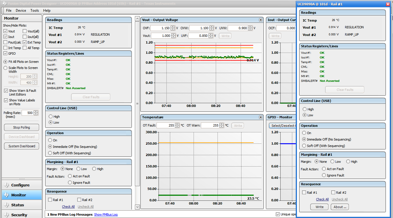 Figure 7-3 Fusion GUI Monitor Page
The UCD9090A also has rail state for each rail to debug the system.
| RAIL STATE | VALUE | DESCRIPTION |
|---|---|---|
| IDLE | 1 | On condition is not met, or rail is shut down due to fault, or rail is waiting for the resequence |
| SEQ_ON | 2 | Wait the dependency to be met to assert ENABLE signal |
| START_DELAY | 3 | TON_DELAY to assert ENABLE signal |
| RAMP_UP | 4 | Enable is asserted and rail is on the way to reach power good threshold. If the power good threshold is set to 0 V, the rail stays at this state even if the monitored voltage is bigger than 0 V. |
| REGULATION | 5 | Once the monitoring voltage is over POWER_GOOD when enable signal is asserted, rails stay at this state even if the voltage is below POWER_GOOD late as long as there is no fault action taken. |
| SEQ_OFF | 6 | Wait the dependency to be met to de-assert ENABLE signal |
| STOP_DELAY | 7 | TOFF_DELAY to de-assert ENABLE signal |
| RAMP_DOWN | 8 | Enable signal is de-asserted and rail is ramping down. This state is only available if TOFF_MAX_WARN_LIMIT is not set to unlimited; or If the turn off is triggered by a fault action, rail must not be under fault retry to show RAMP DOWN state. Otherwise, IDLE state is present. |
The UCD9090A also has status registers for each rail and the capability to log faults to flash memory for use in system troubleshooting. This is helpful in the event of a power supply or system failure. The status registers (Figure 7-4) and the fault log (Figure 7-5) are available in the Fusion GUI. See the UCD90xxx Sequencer and System Health Controller PMBus Command Reference (SLVU352) and the PMBus Specification for detailed descriptions of each status register and supported PMBus commands.
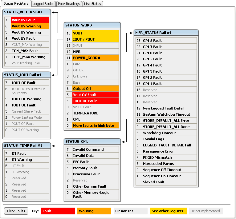 Figure 7-4 Fusion GUI Rail-Status Register
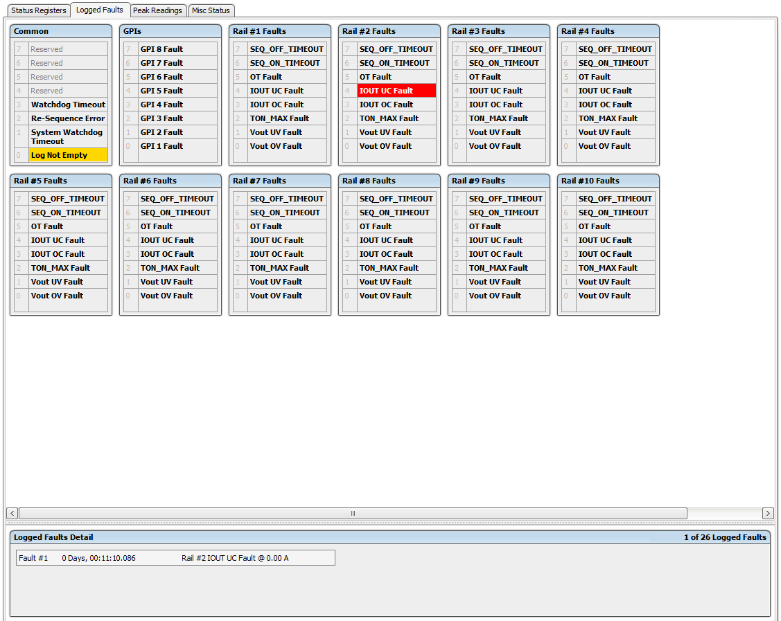 Figure 7-5 Fusion GUI Flash-Error Log (Logged Faults)